Oki OKIFAX 5750 Maintenance Manual
Okifax 5750/5950 facsimile
transceiver
Hide thumbs
Also See for OKIFAX 5750:
- Service manual (1020 pages) ,
- User manual (172 pages) ,
- Maintenance manual (553 pages)

Related Manuals for Oki OKIFAX 5750


Summary of Contents for Oki OKIFAX 5750
- Page 1 OKIFAX 5750/5950 Maintenance Manual 2000-04-20 Rev.2 2000-05-16 Rev.3 Oki Data Corporation 1 / 923 41285901TH Rev.3...
- Page 2 Document Revision History Title: OKIFAX5750/5950 Maintenance Manual Revision Revision Change Item Comments Number Date Author 1999-01 ISSUE E3 Sato 2000-04-20 Add Appendix J. E3 Sato 2000-05-16 Add Appendix K. E3 Endo 41285901TH Rev.3...
- Page 3 PREFACE This manual is intended to be used for installing and maintaining OKIFAX 5750/5950 facsimile transceiver. Maintenance of the OKIFAX 5700/5900 is assumed to be conducted at the following levels: • Assembly-level maintenance for mechanical portions • Unit-level maintenance for electrical at portions CAUTION: DANGER OF EXPLOSION IF BATTERY IS INCORRECTLY REPLACED.
-
Page 4: Table Of Contents
Contents 1. GENERAL INFORMATION ................10 General Performance ......................10 General User’s Functions ....................13 General Maintenance Functions ..................16 General Appearance ......................18 Basic Performance Specifications ..................20 Reports and Lists ......................31 1.6.1 Configuration Report (List of Setting) ..............31 1.6.1.1 Difference From OKIFAX5700/5900 ............ - Page 5 2. INSTALLATION PROCEDURE ............... 107 A. Setup Information..................107 General ........................... 107 Site Selection ........................109 Unpacking ........................111 Contents Identification ....................113 Installation of Attachments ....................114 AC Cord Connection ....................... 119 Telephone and Line Connection ..................120 Pcking for Shipment ......................120 B.
- Page 6 Fundamentals of the Electro-Photographic Process ............264 Actual Electo-photographic Process ................266 Boards and Units ......................267 Overall Dimension and Mechanical Structure of OKIFAX 5750/5950 ......268 4. MECHANICAL DISASSEMBLY AND REASSEMBLY ........270 Precautions for Parts Replacement ................270 Tools ..........................
- Page 7 6.19.1 G3 Service Code List ..................328 6.19.2 G4 Service Code Lists ..................331 6.19.3 Internet-Fax Service Code List ................334 7. TROUBLESHOOTING AND REPAIR FOR OKIFAX 5750/5950 ....336 Overall Troubleshooting Flow Chart ................338 No LCD Operation ......................339 Alarm LED On .........................
- Page 8 7.11 LED Test ......................... 350 7.12 Tone Send Test ....................... 351 7.13 High-speed Modem Test ....................352 7.14 MF Send Test ........................354 7.15 Tone (TEL/FAX) Send Test ....................355 7.16 No Acoustic Line Monitor ....................356 7.17 Power Supply Unit ......................357 7.18 No Document Feeding ....................
- Page 9 Appendix C CIRCUIT DIAGRAMS AND PARTS LIST ........525 Appendix D MECHANICAL EXPANDED VIEW DRAWING AND PARTS LIST 688 Appendix E BOARD LAYOUT OKIFAX 5750/5950 ........704 Appendix F SECOND PAPER FEEDER MAINTENANCE MANUAL ..... 733 Appendix G PC-LOADING ................752 Appendix H RMCS SYSTEM MANUAL (For Model 30) ........
-
Page 10: General Information
• 128 mm to 356 mm Length setting: Long documents (1500 mm) are also available. (7) Automatic document feeder (ADF) • 50 sheets (NA Letter/A4-size: 20-lb/75gm Oki Data recommended paper) • 30 sheets (NA Letter/A4-size: 16 to 28-lb/60 to 105gm) (8) Recording paper •... - Page 11 (12) Scanning resolution a) Horizontal: • 300 dot per inch Note: 600 dpi x 15.4 mm (600 dpi x 600 dpi)*; copy is available. * In case 8 MB option memory is installed. b) Vertical: • 300 dot per inch, 15.4, 7.7, and 3.85 lines per mm Note: 300 dpi x 300 dpi (600 dpi x 600 dpi)*;...
- Page 12 (20) Transmission speed • 2.5 sec. per sheet of ITU-T No.1 evalution test chart (for OKIFAX 5950) • 3.0 sec. per sheet of ITU-T No.1 evalution test chart (for OKIFAX 5750) Note: This is Phase C at 3.85 line/mm and 33.6 kbps.
-
Page 13: General User's Functions
(3) Delayed feeder transmission (4) Memory transmission • 40 sessions (5) Delayed memory transmission (within 3 days) • 20 specified times for OKIFAX 5750 • 30 specified times for OKIFAX 5950 (6) Sequential broadcast (Memory) • 150 stations for OKIFAX 5750 •... - Page 14 (9) Automatic alternate selecting call (FAX No. + FAX No. can be registerd in one-touch keys). • OKIFAX 5750: Speed Dial (1 to 40) are assigned to one-touch keys. • OKIFAX 5950: Speed Dial (1 to 80) are assigned to one-touch keys.
- Page 15 In case of 8 dot/mm x 3.85 lines/mm → 300 dot/inch x 784 lines/inch (15) Auto dialing • Speed dialing: OKIFAX 5750; 1 to 140 (1 to 40 are assigned to one-touch keys.) OKIFAX 5950; 1 to 230 (1 to 80 are assigned to one-touch keys.) • Group dialing; 20 groups •...
-
Page 16: General Maintenance Functions
(3) Phone directory (4) Group directory (5) Activity report (6) Active memory files (7) Broadcast MCF (Message Confirmation) (8) Protocol dump (G3 and G4) (9) NIC configuration (10) Log. report (Service bit = ON) (11) G4 Log. report (Service bit = ON) (12) G3 Log. - Page 17 (7) MF tone test (When NCU board is installed.) (8) Tone (TEL/FAX) test (When NCU board is installed.) (9) Loop back 1 (When ISDN option board is installed.) (10) Loop back 2 (When ISDN option board is installed.) (11) INFO0 sending (When ISDN option board is installed.) (12) INFO1 sending (When ISDN option board is installed.) (13) INFO2 sending (When ISDN option board is installed.) (14) INFO3 sending (When ISDN option board is installed.)
-
Page 18: General Appearance
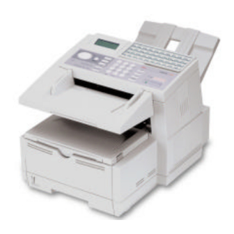
General Appearance Figure 1.4.1 shows the general appearance of the OKIFAX 5750/5950. Stacker-Document Operation Panel Tray-Document Tray-Paper Figure 1.4.1 General Appearance of OKIFAX 5750/5950 18 / 41285901TH Rev.3... - Page 19 Figure 1.4.2 Control Panel of OKIFAX 5750/5950 19 / 41285901TH Rev.3...
-
Page 20: Basic Performance Specifications
Basic Performance Specifications Table 1.5.1 shows basic performance specifications: Table 1.5.1 Basic Performance Specifications Item Specifications Applicable line 1) PSTN (Public switched telephone network) 2) PBX (Private branch exchange ) 3) ISDN (Integrated services digital network): Option 4) FAX2NET Internet Fax (via PSTN): Option 5) E-mail Internet Fax (via LAN): Option Line interface 600 ohm balanced... - Page 21 3) Weight, thickness and condition: Same as above Note: One single sheet should be loaded on the manual paper feeder for one occation. For best results use Oki Data recommended papers 1) Xerox 4200 (20-lb/75gm base weight paper) 21 /...
- Page 22 Item Specifications Recording paper cassette Up to 250 sheets/cassette First cassette (Oki Data recommended paper) Second cassette (option) Up to 500 sheets/cassette (Oki Data recommended paper) Effective recording paper Printing area Recording paper feeding direction 1) Printable area Printable area...
- Page 23 Item Specifications 2) Guaranteed printing area Guaranteed printing area 14 inch 13 inch Letter Size A4 Size Legal Size Legal Size inch inch inch inch 279.4 11.7 355.6 13 330.2 8.27 210 10.5 266.7 11.2 284.3 13.5 342.9 12.5 317.5 203.2 7.77 197.3 203.2...
- Page 24 LCD display will show “MSG. IN MEMORY”, and the Alarm LED turn on. Minimum scan line time for 0 ms, when receiving in ECM mode of from an Oki receiving Data facsimile. 5 ms at 15.4 line/mm or 7.7 line/mm and 10 ms at 3.85 line/mm when receiving from a non-Oki Data facsimile or non-ECM mode.
- Page 25 The modem automatically selects transmission speed according to the line condition. 1) ITU-T Rec. T.30 Protocol 2) Oki special protocol (speed protocol) The T.30 handshaking procedure will be conducted at message transmission speed instead of 300 baud, during transmission multi-page.
- Page 26 Specifications 2.5 seconds at 33.6 kbps with JBIG for OKIFAX 5950 Image transmission time and 3.0 seconds at 33.6 kbps for OKIFAX 5750 per sheet of ITU-T No.1 evaluation test chart. Note: This speed denotes the time interval corre- sponding to Phase C (message transmission phase) as referred to in ITU-T T.30.
- Page 27 Note1: Hardware is standard and software is option for Bi-Centro interface. Note2: For details, see Product Spec. “MFP PC Interface Kit”. • This function can be used for OKIFAX 5750/5950 network printer service. The OkiHSP NIC (Network Network print kit (option) Interface Card) Ethernet Adapter used for OKIFAX...
- Page 28 Item Specifications • Installing the NIC card for OKIFAX 5750/5950 provides Network print service as an option. 1) Network 3.1x, 4.1x 2) TCP/IP 3) Windows NT/95/98/3.1 4) T600dpi, 10 ppm Note: For details, see Product Spec. “Network Print Service” This function can be used when Option LAN board is Internet FAX Kit: E-mail type installed.
- Page 29 8-MB option memory mounted. Note: For details, see Product Spec. “ 600dpi Com- munication”. • G4 communication supports Oki mode relay broad- Relay Broadcast Function cast only. • G3 communication supports both Oki mode relay broadcast and F code relay broadcast.
- Page 30 Item Specifications Ambient condition Temperature and Humidity In operation Power off mode During Storage Unit °F Temperature 32 - 110 14 - 110 50 - 90 (0 - 43) (-10 - 43) (°C) (10 - 32) Humidity 10 - 90 10 -90 20 - 80 °F...
-
Page 31: Reports And Lists
Reports and Lists This section presents the formats of reports and lists referred in the preceeding paragraphs, with some example for reference purpose for US/CANADA/INT’L version. Brief descriptions for the items and sample data are given for the reader’s convenience in understanding the meaning and purpose thereof, except for those which are seemed self explanatory. -
Page 32: Difference From Okifax5700/5900
1.6.1.1 Difference From OKIFAX5700/5900 (*1 to *7 coincide with the notes on the example of the report image.) *1 To be described when ISDN/G3 option is installed. *2 Added descriptions due to the addition of relay broadcasting station function. *3 To be described only when G3 option is installed. *4 To be described when either TYPE1 or TYPE2 of NIC card is installed. -
Page 33: Report Image
1.6.1.2 Report Image CONFIGURATION P1 12/24/2000 22:00 ID=ODC TAKASAKI USER FUNCTION SETUP MACHINE SETTINGS < 10 > AUTO ANSWER MODE < 11 > MONITOR VOLUME HIGH-MID. < 12 > BUZZER VOLUME < 13 > USER LANGUAGE ENGLISH < 14 > REMOTE DIAGNOSIS <... - Page 34 CONFIGURATION P2 12/24/2000 22:00 ID=ODC TAKASAKI USER FUNCTION SETUP REPORT OPTIONS < 70 > MCF. (SINGLE-LOC.) < 71 > MCF. (MULTI-LOC.) < 72 > MESSAGE IN MCF. < 73 > ERR. REPORT (MCF.) LAN OPTIONS < 80 > AUTO TRAY SW <...
- Page 35 CONFIGURATION P3 12/24/2000 22:00 ID=ODC TAKASAKI TECHNICAL FUNCTION SETUP < 01 > SERVICE BIT < 02 > MONITOR CONT. < 03 > COUNTRY CODE < 04 > TIME/DATE PRINT < 05 > TSI PRINT < 06 > TAD MODE TYPE2 <...
-
Page 36: Function List
1.6.2 Function List Method: This list can be printed out manually from the report operation. The list is printed out user function only and does not print technical function. 1.6.2.1 Difference from OKIFAX5700/5900 (*1 to *12 coincide with the notes on the example of the report image.) *1 To be described when LAN option (TYPE2) is installed, or if the Account No. -
Page 37: Report Image
1.6.2..2 Report Image FUNCTION LIST P1 12/24/2000 22:00 ID=0dc Takasaki TO ACCESS PROGRAM MENU ITEMS: -PRESS THE MENU KEY -TO LOCATE A MENU ITEM, USE THE UP-DOWN ARROW KEY -SELECT THE MENU ITEM USING EITHER THE ENTER OR RIGHT ARROW KEYS TO QUICKLY ACCESS A SPECIFIC "SETUP"... - Page 38 FUNCTION LIST P2 12/24/2000 22:00 ID=0dc Takasaki MENU SETUP CLOCK ADJUSTMENT < 00 > CLOCK ADJUTMENT ID/PASSWORD PRG. < 01 > TSI/CSI < 02 > TSI/CSI(G3 OPTION) < 03 > SENDER ID < 04 > PERSONAL BOX < 05 > MEM.
- Page 39 FUNCTION LIST P3 12/24/2000 22:00 ID=0dc Takasaki MENU SETUP INCOMING OPTIONS < 60 > INCOMING RING OFF/ON/DRC < 61 > REMOTE RECEIVE OFF/00-99/**/## < 62 > T/F TIMER PRG. 20/35 SEC < 63 > CONTINUOUS TONE ON/OFF < 64 > PC/FAX SWITCH ON/OFF <...
-
Page 40: Help Report
1.6.3 Help Report Output the following new report by pressing HELP key while the device is in standby state. Following this report, output conventional function list. (4 sheets in total) 1.6.3.1 Report Image (Conditions for descriptions) (1) If the line for descriptions is in blank, don’t move up descriptions in the following lines. (Keep the blank line blank.) HELP REPORT 12/24/2000... -
Page 41: Telephone Directory
Descriptions: Five pages for OKIFAX 5750 and eight pages for OKIFAX 5950. Speed Dial: Up to 140 for OKIFAX 5750, up to 230 for OKIFAX 5950 1. Title of the report 2. Date and time when the report was printed 3. - Page 42 TELEPHONE DIRECTORY P1 12/24/1999 17:05 ID=OKI LOCATION ID TEL NO G3-ECHO / G3-RATE / MODE 1 OKI DATA SYS1 LOC# 1234567890123456789012345678901234567890 33.6 ALT# 0101 2 OKI DATA SYS2 LOC# 0002 33.6 ALT# 0102 3 OKI DATA SYS3 LOC# 0003 33.6...
- Page 43 TELEPHONE DIRECTORY P2 12/24/1999 17:05 ID=OKI LOCATION ID TEL NO G3-ECHO / G3-RATE MODE 31 OKI DATA SYS31 LOC# 1234567890123456789012345678901234567890 [12:12] 33.6 ALT# 0010 32 OKI DATA SYS32 LOC# 0010 [12:12] 33.6 ALT# 0010 33 OKI DATA SYS33 LOC# 0010 [17:12] 33.6...
- Page 44 TELEPHONE DIRECTORY P3 12/24/1999 17:05 ID=OKI LOCATION ID TEL NO G3-ECHO / G3-RATE MODE 61 OKI DATA SYS61 LOC# 1234567890123456789012345678901234567890 33.6 62 OKI DATA SYS62 LOC# 0002 33.6 63 OKI DATA SYS63 LOC# 0003 33.6 64 OKI DATA SYS64 LOC# 0004 33.6...
- Page 45 TELEPHONE DIRECTORY P4 12/24/1999 17:05 ID=OKI LOCATION ID TEL NO G3-ECHO / G3-RATE MODE 91 OKI DATA SYS91 LOC# 1234567890123456789012345678901234567890 33.6 92 OKI DATA SYS92 LOC# 0002 33.6 93 OKI DATA SYS93 LOC# 0003 33.6 94 OKI DATA SYS94 LOC# 0004 33.6...
- Page 46 TELEPHONE DIRECTORY P5 12/24/1999 17:05 ID=OKI LOCATION ID TEL NO G3-ECHO / G3-RATE MODE 121 OKI DATA SYS121 LOC# 1234567890123456789012345678901234567890 33.6 122 OKI DATA SYS122 LOC# 0002 33.6 123 OKI DATA SYS123 LOC# 0003 33.6 124 OKI DATA SYS124 LOC# 0004 33.6...
- Page 47 TELEPHONE DIRECTORY P1 12/24/1999 17:05 ID=OKI LOCATION ID TEL NO G3-ECHO / G3-RATE / MODE 1 OKI DATA SYS1 LOC# 1234567890123456789012345678901234567890 33.6 ALT# 0101 2 OKI DATA SYS2 LOC# 0002 33.6 ALT# 0102 3 OKI DATA SYS3 LOC# 0003 33.6...
- Page 48 TELEPHONE DIRECTORY P2 12/24/1999 17:05 ID=OKI LOCATION ID TEL NO G3-ECHO / G3-RATE MODE 31 OKI DATA SYS31 LOC# 1234567890123456789012345678901234567890 [12:12] 33.6 ALT# 0010 32 OKI DATA SYS32 LOC# 0010 [12:12] 33.6 ALT# 0010 33 OKI DATA SYS33 LOC# 0010 [17:12] 33.6...
- Page 49 TELEPHONE DIRECTORY P3 12/24/1999 17:05 ID=OKI LOCATION ID TEL NO G3-ECHO / G3-RATE MODE 61 OKI DATA SYS61 LOC# 1234567890123456789012345678901234567890 33.6 ALT# 0010 62 OKI DATA SYS62 LOC# 0002 33.6 ALT# 0010 63 OKI DATA SYS63 LOC# 0003 33.6 ALT# 0010...
- Page 50 TELEPHONE DIRECTORY P4 12/24/1999 17:05 ID=OKI LOCATION ID TEL NO G3-ECHO / G3-RATE MODE 91 OKI DATA SYS91 LOC# 1234567890123456789012345678901234567890 33.6 92 OKI DATA SYS92 LOC# 0002 33.6 93 OKI DATA SYS93 LOC# 0003 33.6 94 OKI DATA SYS94 LOC# 0004 33.6...
- Page 51 TELEPHONE DIRECTORY P5 12/24/1999 17:05 ID=OKI LOCATION ID TEL NO G3-ECHO / G3-RATE MODE 121 OKI DATA SYS121 LOC# 1234567890123456789012345678901234567890 33.6 122 OKI DATA SYS122 LOC# 0002 33.6 123 OKI DATA SYS123 LOC# 0003 33.6 124 OKI DATA SYS124 LOC# 0004 33.6...
- Page 52 TELEPHONE DIRECTORY P6 12/24/1999 17:05 ID=OKI LOCATION ID TEL NO G3-ECHO / G3-RATE MODE 151 OKI DATA SYS151 LOC# 1234567890123456789012345678901234567890 33.6 152 OKI DATA SYS152 LOC# 0002 33.6 153 OKI DATA SYS153 LOC# 0003 33.6 154 OKI DATA SYS154 LOC# 0004 33.6...
- Page 53 TELEPHONE DIRECTORY P7 12/24/1999 17:05 ID=OKI LOCATION ID TEL NO G3-ECHO / G3-RATE MODE 181 OKI DATA SYS181 LOC# 1234567890123456789012345678901234567890 33.6 182 OKI DATA SYS182 LOC# 0002 33.6 183 OKI DATA SYS183 LOC# 0003 33.6 184 OKI DATA SYS184 LOC# 0004 33.6...
- Page 54 TELEPHONE DIRECTORY P8 12/24/1999 17:05 ID=OKI LOCATION ID TEL NO G3-ECHO / G3-RATE MODE 211 OKI DATA SYS211 LOC# 1234567890123456789012345678901234567890 33.6 212 OKI DATA SYS212 LOC# 0002 33.6 213 OKI DATA SYS213 LOC# 0003 33.6 214 OKI DATA SYS214 LOC# 0004 33.6...
- Page 55 TELEPHONE DIRECTORY 12/24/1999 17:05 ID=OKI LOCATION ID TEL NO G3-ECHO / G3-RATE MODE 1 OKI DATA SYS1 LOC# 1234567890123456789012345678901234567890 33.6 ALT# 0101 50 OKI DATA SYS50 LOC# 0002 33.6 100 OKI DATA SYS100 LOC# 0003 33.6 Telephone Directory (When the destination is registered by SPEED DIAL No. 1, No.50 and No.
-
Page 56: Group Directory
1.6.5 Group Directory Method: This list can be printed out manually for a selected group only (Group #1 to #20) through operation. Description: 1. Title of the list 2. Date and time when the list was printed. 3. Sender ID 4. - Page 57 GROUP DIRECTORY 12/24/1999 17:04 ID=OKI TAKASAKI GROUP NO. #1=OKI DATA SYS1 LOCATION ID LOCATION ID 1 = 1234567890123456789012345678901234567890 2 = 1234567890123456789012345678901234567890 3 = OKI-SHIBAURA 4 = OKI-SHIBAURA 5 = FX-050 6 = FX-175 7 = FX-0175VP-ENHANC 8 = FX-056 9 = OKIFAX450...
- Page 58 GROUP DIRECTORY P1 12/24/1999 17:04 ID=OKI TAKASAKI GROUP NO. #1=OKI DATA SYS1 LOCATION ID LOCATION ID 1 = 1234567890123456789012345678901234567890 2 = 1234567890123456789012345678901234567890 3 = OKI-SHIBAURA 4 = OKI-SHIBAURA 5 = FX-050 6 = FX-175 7 = FX-0175VP-ENHANC 8 = FX-056...
- Page 59 GROUP DIRECTORY P2 12/24/1999 17:04 ID=OKI TAKASAKI GROUP NO. #1=OKI DATA SYS1 LOCATION ID LOCATION ID 141 = KAI-EIGYOU-INTL 142 = KAI-EIGYOU-GBR 143 = KAI-EIGYOU-NOR 144 = KAI-EIGYOU-SWE 145 = KAI-EIGYOU-DEN 146 = KAI-EIGYOU-GER 147 = KAI-EIGYOU-TCH 148 = KAI-EIGYOU-POL...
- Page 60 GROUP DIRECTORY 12/24/1999 17:04 ID=OKI TAKASAKI GROUP NO. #1=OKI DATA SYS1 LOCATION ID LOCATION ID 1 = 1234567890123456789012345678901234567890 50 = 1234567890123456789012345678901234567890 100 = OKI-SHIBAURA Group Directory (When the destination of SPEED DIAL No. 1, No.50,and No.100 is selected by the group designation.) 60 / 41285901TH Rev.3...
-
Page 61: Self Diagnosis Report
1.6.6 Self Diagnosis Report Purpose: To check ROMs, RAMs and Printing function Method: The report will be manually printed out for maintenance purpose. 1.6.6.1 Difference from OKIFAX5700/5900 (*1 to *3 coincide with the notes on the example of the report image.) *1 Option memory is 2MB/4MB/8MB. -
Page 62: Report Image
1.6.6.2 Report Image SELF DIAGNOSIS REPORT 12/24/2000 12:00 ID=0dc Takasaki MAIN BOARD CPU-ROM VERSION aaaa HASH hhhh CPU-RAM PROGRAM1 VERSION aaaa HASH hhhh PROGRAM2 VERSION aaaa HASH hhhh LANGUAGE VERSION aaaa HASH hhhh DEFAULT VERSION aaaa HASH hhhh DEFAULT TYPE MODEM VERSION hhhh... -
Page 63: G3 Protocol Dump
1.6.7 G3 Protocol Dump Purpose: To allow the serviceman to obtain a list of protocol signals transferred between the transmitter and receiver. Method: The report will be manually printed out for maintenance purpose. If the previous communica- tion is G3, G3 communication protocol dump is printed out. If it is G4, the G4 communication protocol dump is printed. - Page 64 PROTOCOL DUMP P1 12/24/2000 19:00 ID=OKI TAKASAKI DATE TIME S,R-TIME DISTANT STATION ID MODE PAGES RESULT 12/24 18:56 00'33" 123456789012345678901234 0000 # PPS_MPS PPS_EOP NSF DIS TRANSMITTED FRAME 00 00 00 00 00 00 00 00 00 00 00 00 00 00 00 00 00 00 00 00...
- Page 65 PROTOCOL DUMP P2 12/24/2000 19:00 ID=OKI TAKASAKI RECEIVED FRAME FF C8 01 00 73 17 22 00 00 00 00 00 00 00 00 00 00 00 00 00 00 00 00 00 00 00 00 00 00 00 00 00 00 00 00 00 00 00 00 00...
-
Page 66: G4 Protocol Dump
1.6.8 G4 Protocol Dump Purpose: To allow the serviceman to obtain a list of protocol signals transferred between the transmitter and receiver. Method: The report will be manually printed out for maintenance purpose. If it is G4, the G4 communication protocol dump is printed out. Descriptions: 1. - Page 67 PROTOCOL DUMP P1 12/24/2000 19:00 ID=OKI TAKASAKI DATE TIME S,R-TIME DISTANT STATION ID MODE PAGES RESULT 12/24 18:56 00'33" OKI SHIBAURA TX-G4 0000 Dch. SETUP CONN-ACK + Bch + DISC REL-C STATUS SETUP-ACK CONN + Bch + Bch. SABM CDCL...
- Page 68 PROTOCOL DUMP P2 12/24/2000 19:00 ID=OKI TAKASAKI CR/CN 00 00 00 00 00 00 00 00 00 00 00 00 00 00 00 00 00 00 00 00 00 00 00 00 00 00 00 00 00 00 00 00...
-
Page 69: Relay Broadcast Confirmation
1.6.9 Relay Broadcast Confirmation Method: The report will be sent out upon return when the distribution is completed. Descriptions: 1. Title of the report 2. Date and time when the report was printed 3. Sender ID 4. Total numbers of pages in particular communication 5. - Page 70 START TIME = 12/24 17:22 TOTAL TIME = 1:22'22" LOCATION ID PAGES RESULT LOCATION ID PAGES RESULT 1=OKIDATA SYS1 2=OKI DATA SYS2 3=OKIDATA SYS3 4=OKI DATA SYS4 5=OKIDATA SYS5 6=OKI DATA SYS6 7=OKIDATA SYS7 8=OKI DATA SYS8 9=OKIDATA SYS9 10=OKI DATA SYS10...
- Page 71 RELAY BROADCAST CONFIRMATION REPORT P2 12/24/2000 19:22 ID=OKI LOCATION ID PAGES RESULT KEYPAD 12345678901234567890 12345678901234567890 12345678901234567890 12345678901234567890 12345678901234567890 12345678901234567890 12345678901234567890 12345678901234567890 12345678901234567890 12345678901234567890 Relay Broadcast Confirmation Report P2 for OKIFAX5750 71 / 41285901TH Rev.3...
- Page 72 START TIME = 12/24 17:22 TOTAL TIME = 1:22'22" LOCATION ID PAGES RESULT LOCATION ID PAGES RESULT 1=OKIDATA SYS1 2=OKI DATA SYS2 3=OKIDATA SYS3 4=OKI DATA SYS4 5=OKIDATA SYS5 6=OKI DATA SYS6 7=OKIDATA SYS7 8=OKI DATA SYS8 9=OKIDATA SYS9 10=OKI DATA SYS10...
- Page 73 12/24/2000 19:22 ID=OKI LOCATION ID PAGES RESULT LOCATION ID PAGES RESULT 141=OKIDATA SYS141 142=OKI DATA SYS142 143=OKIDATA SYS143 144=OKI DATA SYS144 145=OKIDATA SYS145 146=OKI DATA SYS146 147=OKIDATA SYS147 148=OKI DATA SYS148 149=OKIDATA SYS149 150=OKI DATA SYS150 151=OKIDATA SYS151 152=OKI DATA SYS152...
- Page 74 19:22 ID=OKI PAGES = 001 START TIME = 12/24 17:22 TOTAL TIME = 1:22'22" LOCATION ID PAGES RESULT LOCATION ID PAGES RESULT 1=12345678901234567890 50=OKI DATA SYS2 100=OKIDATA SYS3 KEYPAD 12345678901234567890 12345678901234567890 12345678901234567890 12345678901234567890 12345678901234567890 12345678901234567890 12345678901234567890 12345678901234567890 12345678901234567890 12345678901234567890 Relay Broadcast Confirmation Report (When the destination is specified by SPEED DIAL No.1, No.50, No.100, and KEYPAD)
-
Page 75: Internet Fax Reception Error Report (Error Mail Report)
(always output irrespective of the setting). Descriptions of the content of communication are same as for the Reception of Internet FAX of (1), (3)-(5) of “ 1.6.11 Activity Report” ERROR MAIL REPORT 17/02/2000 13:00 ID=Oki Data DATE TIME S,R-TIME DISTANT STATION ID MODE... -
Page 76: Activity Report
4. Total TX and total RX 5. Date of transmission or reception 6. Time when the communication started 7. Length of time for which the OKIFAX 5750/5950 was connected to the line 8. Identification of the remote station Personal ID/CSI (TSI)/Location ID/Dial number/Called TID/Calling TID 9. -
Page 77: Difference From Okifax5700/5900
1.6.11.1 Difference from OKIFAX5700/5900 (1) Describes Internet FAX, Fax2Net Email/WEB address to DISTANT STATION ID. • Character string including the lower-case alphabetic characters and symbols • Leading 24 characters • Describes Speed Dial registered address ID when transmitting Internet Fax, and Fax2Net (Email transmission, Web Retrieval). - Page 78 9082 12/24 10:36 01’10” ODS FUKUSHIMA POLL=01 0000*7 12/24 13:00 01’00” OKI DATA SYS POLL TX 0000 *1: Confidential reception *2: Manual TX *3: Memory reception *4: Broadcast TX *5: G4 TX *6: Polling TX *7: Bulletin poll TX Activity Report 78 / 41285901TH Rev.3...
-
Page 79: Message Confirmation
4. Total TX and total RX time 5. Date of transmission or reception 6. Time when the communication started 7. Length of time for which the OKIFAX 5750/5950 was connected to the line 8. Identification of the remote station Personal ID/CSI(TSI)/Location ID/Dial number/Called TID/Calling TID 9. - Page 80 MESSAGE CONFIRMATION 12/24/2000 17:05 ID=OKI DATE S,R-TIME DISTANT STATION ID MODE PAGES RESULT 12/24 0'20" 123456789012345678901234 0000 IMAGE Message Confirmation (When the transmission is the normal end) 80 / 41285901TH Rev.3...
- Page 81 Printed only when Error page MESSAGE CONFIRMATION 12/24/2000 17:05 ID=OKI DATE S.R-TIME DISTANT STATION ID MODE PAGES RESULT 12/24 0'20" 123456789012345678901234 0000 POSSIBLE ERROR PAGE:*001*002 IMAGE Message Confirmation (Error report) 81 / 41285901TH Rev.3...
-
Page 82: Power Outage Report
1.6.13 Power Outage Report Purpose: To indicate AC power failure and recovery and in case of destruction of accumulated picture data in the memory. the information printed on the Power Outage Report is not printed out on the Activity report. Method: If received communications are lost due to power failure, this report is output automatically at power recovery. - Page 83 DATE TIME S,R-TIME DISTANT STATION ID MODE PAGES RESULT 12/24 10:10 123456789012345678901234 LOST 12/24 10:30 ODS TAKASAKI LOST 12/24 12:05 01'20" OKI FAX CONF=01 LOST 0000 12/24 13:00 00'20" 03-5476-4300 LOST 0000 12/24 10:50 00'20" 0495-22-5400 LOST 0000 12/24 15:00 B.C.
-
Page 84: Confidential Rx Report
3. Sender ID 4. Date of transmission or reception 5. Time when the communication started 6. Length of time for which the OKIFAX 5750/5950 was connected to the line 7. Identification of the remote station 8. Mode of the communication The stored confidential box number is printed in the MODE column. - Page 85 CONFIDENTIAL RX REPORT 12/24/2000 17:05 ID=OKI DATE S,R-TIME DISTANT STATION ID MODE PAGES RESULT 12/24 01'30" 123456789012345678901234 CONF=01 0000 Confidential RX Report 85 / 41285901TH Rev.3...
-
Page 86: Active Memory File
1.6.15 Active Memory File Method: The report will be manually or automatically printed out for information of transmission/recep- tion data stored in the memory. When there is no stored image data in the memory at all, the Active Memory Files is not printed out. Descriptions: 1. -
Page 87: Difference From Okifax5700/5900
1.6.15.1 Difference from OKIFAX5700/5900 (1) Description of Email address or Web URL is enabled to the DISTANT STATION ID column of TRANSMISSION. • Character string containing the lower-case alphabetic characters and symbols • Speed Dial: Descriptions of maximum 24 characters. If exceeding 24 characters, description starts from the top. - Page 88 12/24/2000 19:10 ID=ODS RECEPTION ENTRIES PAGES TRANSMISSION DATE TIME DISTANT STATION ID MODE PAGES 12/24 13:00 OKI DATA SYS-1 12/24 12:03 OKI DATA SYS-2 12/24 13:00 OKI DATA SYS-3 12/24 13:05 OKI DATA SYS-4 12/24 14:00 OKI DATA SYS-5 12/24...
- Page 89 ACTIVE MEMORY FILES P2 12/24/2000 19:10 ID=ODS PERSONAL BOX BOX NO. MODE ENTRIES PAGES CONF CONF CONF CONF POLL POLL POLL POLL POLL POLL POLL POLL POLL POLL POLL POLL Active Memory Files P2 (In case of more than 1 page) 89 / 41285901TH Rev.3...
-
Page 90: Active Memory Files
12/24/2000 19:10 ID=ODS RECEPTION ENTRIES PAGES TRANSMISSION DATE TIME DISTANT STATION ID MODE PAGES 12/24 13:00 OKI DATA SYS-1 12/24 15:30 OKI DATA SYS-9 12/24 15:50 OKI DATA SYS-10 12/24 16:10 OKI DATA SYS-11 12/24 16:30 OKI DATA SYS-12 12/24... -
Page 91: Broadcast Entry Report
1.6.16 Broadcast Entry Report Method: The report will be manually or automatically printed out. Descriptions: 1. Title of the report 2. Date and time when the report was printed 3. Sender ID 4. Required transmission address (Speed dial) 5. Registered location ID 6. - Page 92 BROADCAST ENTRY REPORT P1 12/24/2000 17:04 ID=OKI TAKASAKI LOCATION ID LOCATION ID 1=1234567890123456789012345678901234567890 2=1234567890123456789012345678901234567890 3=OKI-SHIBAURA 4=OKI-SHIBAURA 5=FX-050 6=FX-175 7=FX-175VP-ENHANC 8=FX-056 9=OKIFAX450 10=OKIFAX460M 11=M125INTL 12=M125-US 13=OKIFAX5600 14=OKIFAX1050 15=OKIFAX1000 16=OKIFAX2200 17=OF-3GX 18=115AD 19=2275 20=OF-8 21=OF-18 22=OF-58H 23=M4200 24=5400 25=OF-2B 26=OF-1 27=OF-21 28=2127...
- Page 93 BROADCAST ENTRY REPORT P2 12/24/2000 17:04 ID=OKI TAKASAKI LOCATION ID KEYPAD 1234567890123456789012345678901234567890 1234567890123456789012345678901234567890 1234567890123456789012345678901234567890 1234567890123456789012345678901234567890 1234567890123456789012345678901234567890 1234567890123456789012345678901234567890 1234567890123456789012345678901234567890 1234567890123456789012345678901234567890 1234567890123456789012345678901234567890 1234567890123456789012345678901234567890 Broadcast Entry Report for OKIFAX5750/5950 (2/2) 93 / 41285901TH Rev.3...
- Page 94 BROADCAST ENTRY REPORT P1 12/24/2000 17:04 ID=OKI TAKASAKI LOCATION ID LOCATION ID 1=1234567890123456789012345678901234567890 2=1234567890123456789012345678901234567890 3=OKI-SHIBAURA 4=OKI-SHIBAURA 5=FX-050 6=FX-175 7=FX-175VP-ENHANC 8=FX-056 9=OKIFAX450 10=OKIFAX460M 11=M125INTL 12=M125-US 13=OKIFAX5600 14=OKIFAX1050 15=OKIFAX1000 16=OKIFAX2200 17=OF-3GX 18=115AD 19=2275 20=OF-8 21=OF-18 22=OF-58H 23=M4200 24=5400 25=OF-2B 26=OF-1 27=OF-21 28=2127...
- Page 95 159=KAI-SISYA-NOR 160=KAI-SISYA-SWE 161=KAI-SISYA-DEN 162=KAI-SISYA-GER 163=KAI-SISYA-TCH 164=KAI-SISYA-POL 165=KAI-SISYA-AUT 166=KAI-SISYA-BEL 167=KAI-SISYA-FRE 168=KAI-SISYA-ESP 169=KAI-SISYA-GRE 170=KAI-SISYA-AUS 171=KAI-SISYA-SIN 172=KAI-SISYA-HNG 173=OKI DATA USA 174=OKI DATA INTL 175=OKI DATA BGR 176=OKI DATA IRL 177=OKI DATA NOR 178=OKI DATA SWE 221=ABCDEFGHIJ12345 222=ABCDEFGHIJ23456 223=ABCDEFGHIJ34567 224=ABCDEFGHIJ45678 225=ABCDEFGHIJ56789 226=ABCDEFGHIJ67890 227=ABCDEFGHIJ78901 228=ABCDEFGHIJ89012...
-
Page 96: Broadcast Entry Report
BROADCAST ENTRY REPORT 12/24/2000 17:04 ID=OKI TAKASAKI LOCATION ID LOCATION ID 1=1234567890123456789012345678901234567890 50=1234567890123456789012345678901234567890 100=OKI-SHIBAURA KEYPAD 1234567890123456789012345678901234567890 1234567890123456789012345678901234567890 1234567890123456789012345678901234567890 1234567890123456789012345678901234567890 1234567890123456789012345678901234567890 1234567890123456789012345678901234567890 1234567890123456789012345678901234567890 1234567890123456789012345678901234567890 1234567890123456789012345678901234567890 1234567890123456789012345678901234567890 Broadcast Entry Report (When the destination of Broadcast TX is specified by SPEED DIAL No.1, No.50, and No.100) 96 / 41285901TH Rev.3... -
Page 97: Broadcast Confirmation Report
ID=ODC PERSONAL BOX = 10 LOCATION ID LOCATION ID 1 = 1234567890123456789012345678901234567890 10 = OKI DATA 20 = ODS 1.6.19 G3 Log Report Newly outputs debug log information by the firm of G3 option board. Report format is identical with MCNT and the log information by the firm of G4 option. -
Page 98: Nic Configuration
1.6.20 NIC Configuration Refer to the “Internet FAX System Specifications.” NIC CONFIGURATION (TYPE 1 OEL Version) 09/22/2000 16:54 ID=OKIDATA CORP.E8S (FAX&MFP S/W) MLETB08 Version 1.0.2 TCP/IP status IP address : 202.250.103.63 Subnet Mask : 255.255.255.0 Gateway addr : 202.250.103.254 NetWare status NWPrint mode: PSERVER Packet type : 802.3 Metwork no. - Page 99 NIC CONFIGURATION (TYPE 1 ODA Version) 09/14/2000 11:54 ID=OKIDATA CORP.E8S (FAX&MFP S/W) +----------------------------------------------------------------------------------+ General Infomation +----------------------------------------------------------------------------------+ Network Card Name : OkiLAN 7100e+ MAC Address : 0080921E63FE Firmware Version : 1.1.0 Link Status : OK (10BASE-T Half) Network Status Unicast Packets Received : 153 Packets Transmitted : 16879 Total Packets Received : 460613...
- Page 100 NIC CONFIGURATION (TYPE 2) 09/22/2000 16:54 ID=OKIDATA CORP.E8S (FAX&MFP S/W) 100 / 41285901TH Rev.3...
-
Page 101: Nic Information
1.6.21 NIC Information 101 / 41285901TH Rev.3... -
Page 102: E-Mail Maintenance Report
1.6.22 E-mail Maintenance Report E-mail Maintenance Function When EMAIL MAINTENANCE=ON (Setting by service personnal), e-mail is transmitted at 00:00 a.m. every day the following image format. 12/24/1999 12:00 PERSONAL ID =0dc Takasaki TEL NO. =609-222-1234 TEL NO.(G3 OPTION) =609-333-4567 MAIN BOARD CPU-ROM VERSION aaaa... -
Page 103: Descriptions Of Communication Mode Column
1.6.23 Descriptions of Communication Mode Column 1.6.23.1 Mode Column in Activity Report I-FAX F2N (Email) F2N (G3) Communication TX-G4 IFAX-TX FNET POLL-TX POLL TX *1 POLL TX-G4 *1 Bull. POLL TX — Bull. POLL TX(BOX) POLL=XX POLL=XX-G4 Broadcast TX-G4 BC-IFAX *3 FNET Relay Broadcast REL-T=XX... -
Page 104: Output Conditions Of Various Mcf Reports During Transmission
1.6.24 Output Conditions of Various MCF Reports During Transmission 1.6.24.1 Difference from OKIFAX5700/5900 • Describes the results of broadcast transmission to respective addresses to the Activity Report. • One-line description of “MODE=B.C. RESULT=COMP” used to be made to the Activity Report is cancelled. -
Page 105: Reports To Be Output Upon Canceling Communication By Pressing Stop Key
1.6.24.3 Reports to be output upon canceling communication by pressing STOP Key Setting Automatic Output Report Image in MCF Setting Item Described together ERR. BROADCAST with MCF (MULTI) (SINGLE) (MULTI) Each Address (with picture) with picture Broadcast of — (B.C.STOP) —... -
Page 106: Reports To Be Output When The Communication Is Completed Normally
1.6.24.5 Reports to be output when the communication is completed normally. Setting Automatic Output Report Image in MCF Setting Item Described together ERR. BROADCAST with MCF (MULTI) (SINGLE) (MULTI) Each Address (with picture) with picture — Broadcast communication (During address transmission) —... -
Page 107: Installation Procedure
INSTALLATION PROCEDURE Setup Information General The following flowchart outlines the installation procedure. Site selection (See 2.2) Unpacking (See 2.3) Contents identification (See 2.4) Installation of attachments (See 2.5) AC cord connection (See 2.6) Telephone and line connection (See 2.7) Packing for shipment (See 2.8) General procedure key operation (See 2.9.1) - Page 108 Off-line tests (See 2.9.9) On-line tests (See 2.9.10) Installation of optional units (See 2.10) #1: For operation and registration, see OKIFAX 5750/5950 Handbook. #2: Memory board, G4 option board, LAN option board, Second cassette unit etc.,. 108 / 41285901TH Rev.3...
-
Page 109: Site Selection
Site Selection INSTALLATION Precautions for Installation (1) Fluctuation in line voltage • 120VAC (102V to 127V) • 230VAC (198V to 264V) (2) Room temperature • 50 to 90°F (10 to 32°C) (3) Humidity • 20 to 80% RH (4) Operating environment •... - Page 110 Document exit Document Paper exit (face down) Paper exit (face up) Recording paper cassette Paper 11.81" 19.69" (300mm) (500mm) Note: *1: This space necessary for having the telephone set. *2: This space is necessary for removing the recording paper cassette. *3: This space is necessary for installing the document stacker and allow space for the fan exhaust.
-
Page 111: Unpacking
Unpacking Procedure (1) Remove the on the top of the carton box and open its cover. External carton box Packing tape Packing tape Carton label Figure 2.3.1 Unpacking Procedure (1) (2) Take out the accessory box from the carton box. (See figure 2.3.2) (3) Take out the machine with plastic wrapper from the box. - Page 112 Box-Accessories Connecting Codes Toner Cartrige Stacker Document OKIFAX 5750/5950 Pad-Assy (L) 40932401 Pat-Assy (R) 40932402 Box-Individual Bar Code Figure 2.3.2 Unpacking Procedure (2) 112 / 41285901TH Rev.3...
-
Page 113: Contents Identification
After having taken out the machine and accompainied accessaries from the carton box, check the contents according to the following list. Table 2.4.1 Contents List Item No. Name Q’ty Remarks OKIFAX 5750/5950 facsimile AC power cord I/D unit Already installed. Toner cartridge Document stacker Telephone line code One touch sheet Already installed. -
Page 114: Installation Of Attachments
Installation of Attachments (1) Items • Image Drum (ID) Unit (already installed) • Toner cartridge • Recording paper • Document stacker (2) Procedure 1) Toner cartridge • Peel off the fixed tape attached to the tray-paper. • Open the tray-document and tray-paper. Figure 2.5.1 Toner Cartridge Installation (1) •... - Page 115 • Take out the toner cartridge from the damp proof bag, shake it five or six times as shown in the illustration to eliminate the toner deflection, and peel off the seal gently. Seal Toner cartridge Figure 2.5.3 Toner Cartridge Installation (3) •...
- Page 116 • Press the gray lever forward until it stops. Figure 2.5.5 Toner Cartridge Installation (5) • Clean the toner scattered in the vicinity of the toner cartridge using a cloth moist- ened with cold water. Do not use hot water since it makes the toner stick there. •...
- Page 117 2) Recording paper Note: About 250 sheets of the new paper can be set in the recording paper cassette. • Remove the paper cassette from the facsimile by pulling the cassette tab. • Sheets must not exceed the paper full marker of the new paper limit indication. If excessive sheets are set, it will cause paper jams.
- Page 118 3) Document stacker • Hang the document stacker onto hanging position. 118 / 41285901TH Rev.3...
-
Page 119: Ac Cord Connection
AC Cord Connection The power supply is provided as follows: Normal input voltage 120VAC (Voltage range 102 to 127VAC) Normal input voltage 230VAC (Voltage range 198 to 250VAC) Check whether the AC voltage of your input is within the above-mentioned voltage range and if so, check that the power switch is turned OFF. -
Page 120: Telephone And Line Connection
Exchange line External telephone cable Pcking for Shipment Caution: When packing the OKIFAX 5750/5950 for shipment, REMOVE THE IMAGE DRUM AND TONER FROM THE UNIT AND SHIP SEPARATELY! Failure to do this will result in damege to the machine. 120 /... -
Page 121: Programming And Initial Settings
Programming and Initial Settings Initial Settings 2.9.1 General Procedure of Key Operation Note: The fonts displayed on the LCD operation panel may differ from the fonts written this manual. Accessing to desired functions: • There are two methods for accessing a desired function: Step access and Speed access (direct access). - Page 122 User functions MENU Delayed TX Note: Delayed Batch TX Options preceded by a number in permit speed Priority TX access. Other options do not permit speed access. Confidential TX Relayinitiate TX Internet FAX Internet TX Internet TX Polling TX/RX Polling TX Bulletin Poll (BOX) Memory Poll Memory Poll (BULL)
- Page 123 Machine Settings Auto Answer Mode Monitor Volume Buzzer Volume User Language Remote Diagnosis Tx Mode Default No Toner Mem. Rx Mem. Full Save Instant Dial Restrict Access ECM Function Closed Network Toner Save Sender ID 1'st Paper Size 2'nd Paper Size Power Save Mode Relay Print 600dpi Function...
- Page 124 Report Options MCF (Single-Loc.) MCF (Multi-Loc.) Image in MCF. Err. Report (MCF.) LAN Options AUTO TRAY SW. PAPER SIZE CHECK LAN PRINT T.O. POP INTERVAL DEL RECEIVED MSG. TIME BETWEEN GMT TEXT PRINT HEADER PRINT CODING MODE EX.FINE MODE IFAX SENDER ID DOMAIN NAME NETWORK SETTINGS IP ADDRESS...
- Page 125 Technical functions MENU RESOLUTION key x 2 Local Test Self Diagnosis Sens. Calibration LED Test Tone Send Test Modem Send Test Modem Rec. Test MF(Tone) Test Tone(T/F) Test LOOP BACK 1 LOOP BACK 2 INFO0 SENDING INFO1 SENDING INFO3 SENDING PULSE (1KHZ) SEND PULSE (2KHZ) SEND PULSE (N2KHZ) SEND...
- Page 126 Print Priority Relay Broadcast FAX2NET Function JBIG Facility LLC Check G3/G4 Learning G3 Setup BC Gateway Service Email Maintenance Admin Email Addr. Command T.O. System Reset All Data CLR Location Data CLR Config. Data CLR Default Type Set PC Loading G4 PC Loading G3 PC Loading 126 /...
-
Page 127: Technical Functions: Setup
2.9.2 Technical Functions: Setup 1. This section explains items generally conducted by service personnel, not by users. (1) Step access 1) The machine is standby state with no document. 2) Press the MENU/EXIT key once. 3) Press the RESOLUTION key twice. The display will be shown the “TECHNICAL PRG.”. -
Page 128: Technical Functions Operation 1
2.9.2.1 Technical Functions Operation 1 Select Menu is shown as below: 1. Local Test 2. Technical Setup: Go to Section 2.9.2.2 3. System Reset 4. Default Type Set 5. PC Loading 6. G4 PC Loading or G3 PC Loading *2 This mode can be selected when G3 option is installed. M E N U 6 P O L L I N G T X / R X 7 >... -
Page 129: Technical Functions Operation 2
2.9.2.2 Technical Functions Operation 2 Setup 01: Service Bit (OFF/ON) 02: Monitor Cont. (OFF/ON) 03: Country Code (selecting the country code) 04: Time/Date Print (OFF/ONCE/ALL) 05: TSI Print (OFF/ON) 06: TAD Mode (OFF/TYPE1/TYPE2/TYPE3) 07: Real Time Dial (OFF/TYPE1/TYPE2) 08: TEL/FAX Switch (OFF/ON) 09: MDY/DMY (Month/Day/Year or Day/Month/Year) - Page 130 T E C H N I C A L P R G . T E C H N I C A L P R G . X X <Speed Access> 1 L O C A L T E S T 1 >...
- Page 131 ↑ ↓ → ENTER/ S E T U P 0 8 T E L / F A X S W I T C H "08" 0 7 R E A L T I M E D I A L > O F F 0 8 >...
- Page 132 ↑ ↓ → ENTER/ "15" S E T U P 2.9.2.2.2 T1(RX) TIMER VALUE 1 4 T 1 ( T X ) T I M E R V A L U E 1 5 > T 1 ( R X ) T I M E R V A L U E 1 6 T 2 T I M E R * 1 0 0 M S ↑...
- Page 133 ↑ ↓ → ENTER/ S E T U P "22" 2.9.2.2.6 T/F TONE ATT. 2 1 A T T E N U A T O R 2 2 > T / F T O N E A T T . 2 3 M F A T T .
- Page 134 ↑ ↓ → ENTER/ S E T U P 2 9 V 3 4 T X R E T R Y "29" 2 8 T R L A T C H C U R R E N T > O F F 2 9 >...
- Page 135 ↑ ↓ → ENTER/ S E T U P 3 6 R E L A Y B R O A D C A S T "36" 3 5 P R I N T P R I O R I T Y >...
- Page 136 ↑ ↓ S E T U P 4 3 E M A I L M A I N T E N A N C E → "43" ENTER/ 4 2 G A T E W A Y S E R V I C E >...
-
Page 137: T1 (Tx) Timer Value
2.9.2.2.1 T1 (TX) Timer Value Set the T1 timer (call connection wait time: XTTO) for transmission. S E T U P T E C H N I C A L P R G . 1 4 1 3 H / M O D E M R A T E 1 >... -
Page 138: T1 (Rx) Timer Value
2.9.2.2.2 T1 (RX) Timer Value Set the T1 timer for reception. The time from issue of the first DIS to issue of a signal is checked. If a time-out occurs, the line is disconnected. S E T U P T E C H N I C A L P R G . 1 5 1 4 T 1 ( T X ) T I M E R V A L U E 1 >... -
Page 139: T2 Timer *100Ms
2.9.2.2.3 T2 Timer *100ms Registers the time duration (in seconds) for which the fax detects the EOL interval during reception of phase C. The fax disconnects the line when EOL can not detect within T2 Timer. S E T U P T E C H N I C A L P R G . -
Page 140: Error Criterion
2.9.2.2.4 Error Criterion Registers the threshould value whether to transmit RTN or MCF signal when the error occurs in received data. S E T U P T E C H N I C A L P R G . 1 8 1 7 D I S B I T 3 2 1 >... -
Page 141: T/F Tone Att
2.9.2.2.6 T/F Tone Att. Adjusts the attenuation (dB) for the quasi-ring back tone send signal of TEL/FAX switching. Adjusting value is 0 to 15dB in one dB steps. S E T U P T E C H N I C A L P R G . 2 2 2 1 A T T E N U A T O R 1 >... -
Page 142: Ring Dura. *10Ms
2.9.2.2.8 Ring Dura. *10ms Selects the minimum ring detection time to meet country's requirements. Adjusting time is 100MS to 990MS in 10MS steps. S E T U P T E C H N I C A L P R G . 2 4 2 3 M F A T T . -
Page 143: Led Headstrobe
2.9.2.2.10 LED Headstrobe Setting of LED print head strobe signals (00000 - 11111). Selection of strobe sidth in LED head. "00000" is lightest and "11111" is darkest. S E T U P T E C H N I C A L P R G . 2 6 2 5 C M L T I M I N G * 1 0 0 M S 1 >... -
Page 144: Admin Email Addr
2.9.2.2.11 ADMIN Email Addr. S E T U P T E C H N I C A L P R G . 4 3 4 3 E M A I L M A I N T E N A N C E 1 >... -
Page 145: Technical Functions (Setup)
2.9.2.3 Technical Functions (Setup) • Table 2.9.2.3 shows the initial setting items and their purpose. (The default setting is different by the individual countries.) • Each item can be accessed by entering it on Technical Setup. • The detailed procedures of the initial settings items will be explained on the following tables. The setting data must be transferred to the G3 Option side. - Page 146 Table 2.9.2.3 Technical Functions: Setup (2/11) Item Specifications TSI Print Determine whether a TSI is to be printed in the received image. 1) Setting value ON (Printed)/OFF (Not printed) * When this setting is ON and TIME/DATE PRINT is set to ALL , a TSI is printed on all received pages.
- Page 147 Table 2.9.2.3 Technical Functions: Setup (3/11) Item Specifications Real Time Dial Determine whether real-time dialing is enabled. If it is enabled, determine when it will be enabled. 1) Setting values OFF/TYPE1 (External telephone is off-hooked)/TYPE2 OFF: Real-time dialing is disabled (accumulated dialing only) TYPE1: Enabled when the external telephone is off-hooked.
- Page 148 Table 2.9.2.3 Technical Functions: Setup (4/11) Item Specifications MH Only Determine whether only MH coding is to be handled forcibly. This setting is required when the line noise affects the received image. 1) Setting values ON (MH only)/OFF (JBIG; only OKIFAX5950, MMR, MR, or MH is selected depending on communication capacity) H/MODEM Rate Set the initial value of modem transmission speed.
- Page 149 Table 2.9.2.3 Technical Functions: Setup (5/11) Item Specifications DIS Bit32 Determine whether the thirty-second bit (expansion bit) and the succeeding bit 32 of DIS is to be sent out. 1) Setting values ON (Transmits a bit 32)/OFF (Not transmit) * When OFF is selected, machines of other companies cannot receive documents in the EX.FINE, SEP/SUB mode or JBIG.
- Page 150 Table 2.9.2.3 Technical Functions: Setup (6/11) Item Specifications T/F Tone Attenuator Set the T/F pseudo ring back tone signal attenuator (level). (for TEL/FAX switch) 1) Setting values 0-15 dB (in 1 dB steps) * Enter a value with ten-keys. MF Attenuator [Set the MF signal attenuator (level).
- Page 151 Table 2.9.2.3 Technical Functions: Setup (7/11) Item Specifications LED Head Strobe Set the LED head strobe time. The larger the value, the darker the image. 1) Setting values 00000 to 11111 (5 bits) Note 1: When the rank marking of the new replaced LED print head (new part) is same as that of the old used LED print head (old part), you do not always have to set the LED print head strobe signal.
- Page 152 ON (sent)/OFF (Not sent) * If data is transmitted with this setting OFF, DCS transmis- sion is performed (NSC is not sent) even if the Oki NSF is received. * If REMOTE DIAGNOSIS is set to ON although NSF Switch (this setting) is set to OFF, an NSF is sent and sent immedi- ately if Oki’s original function is ON (confidential, etc.).
- Page 153 Table 2.9.2.3 Technical Functions: Setup (9/11) Item Specifications Toner Count Clear Determine whether the toner counter can be cleared regardless of the service bit setting (ON/OFF). 1) Setting values ON (Can be cleared)/OFF (Cannot be cleared) Display Counter display Counter clear clear Service bit Service bit...
- Page 154 Table 2.9.2.3 Technical Functions: Setup (10/11) Item Specifications FAX2NET FUNCTION Sets up whether to make FAX2NET related operation. 1) Setting value ON: FAX2NET related operation is allowed. OFF: All FAX2NET setting and operation cannot be displayed and printed. * When FAX2NET communication is the wait state, change of setting is inhibited.(FUNC NOT AVAIL.) JBIG Facility Set up the encoding JIG.
- Page 155 Table 2.9.2.3 Technical Functions: Setup (11/11) Item Specifications ADMIN EMAIL ADDR. Registers Email address of FAX administrator. To be used for the address when FAX sends any information to the administrator via Email. 1) Email Address of administrator registration number of digits 64 digits (Input-enabled characters are same as Email Address) * Setting enabled only when NIC TYPE2 (IFAX enabled) is...
-
Page 156: Tel/Fax Automatic Switching
2.9.2.4 TEL/FAX automatic switching This function is used for the purpose of TEL/FAX automatic switching as follows. 1) If the machine detects a call with a CNG signal indicating an auto send facsimile call, it starts an automatic document receiving operation. 2) If machine detects a call without a CNG signal, machine generates the buzzer sounds as a telephone call. - Page 157 (20/35 sec) LIFT HANDSET PRESS STOP TO CANCEL Load document NSF, CSI, DIS Press START Button AUTO REC. START Manual OKI TOKYO Transmission PAGE 001 RECEIVING G3/33.6K CML"OFF" 1 sec 1 sec 3.2 sec To detect CNG signal Notes *1:Ring Back Tone — 1 sec. ON, 3.2 sec. OFF *2:When you want to talk by phone, pick up handset.
-
Page 158: Tad Mode
2.9.2.5 TAD mode • TAD: Telephone Answering Device • TAD can be connected to extenal telephone terminal to record your messages. • TAD records your speech and switches an automatic voice message response to the calling station. Note1: A choice of TAD mode is available by technical Function (Setup No.06). Note2: The predetermined time is selectable between 20 or 35 sec. - Page 159 • TAD mode flow chart 1) In case of TYPE2: If the fax does not CNG signal during working of TAD, the fax will go to standby state. 2) In case of TYPE 3: The fax does not detect CNG signal during 15 seconds from TAD operation starting. The fax starts CNG signal detection after 15 seconds from TAD operation.
-
Page 160: Outline Of Parallel Pick Up
The two possible parallel connections of telephone sets A and B are shown in the figure. Remote control FAX (OKIFAX 5750/5950 etc.) To Modem Line Remote control: To control a fax from telephone set A Parallel Pick Up (PP): To control a fax from telephone set B. - Page 161 (1/2) TEL1 S1.1~2 OFF-HOOK TEL2 Detector ’ (2/2) I SW S1 - 3~6 Ring Detector " Impedance C31 R590 matching CN15 ~ Loop CN45 Current Detection MUTE LINE , AR arresters to Modem MF 2-digit Receiving special code CML: ON sensitivity MUTE circuit...
-
Page 162: User's Functions
2.9.3 User’s Functions This section explains the items usually set up by general users. • Select Menu is shown as below: 1. Delayed TX 2. Delayed Batch TX 3. Priotity TX 4. Confidential TX 5. Relayinitiate TX 6. Internet TX 7. - Page 163 Menu selection Given below are the sections to refer to when selecting user functions. 1 2 : 0 0 F A X 1 0 / 0 1 / 1 9 9 8 1 2 : 0 0 F A X Document on hopper MENU S E L E C T L O C A T I O N ( S )
-
Page 164: Location Program
2.9.4 Location Program 1) The machine is standby state with no document. 2) Press the MENUEXIT key once. 3) Press the SHIFT DOWN (↓) key two times. 4) The menu option “9 LOCATION PROGRAM” indicated by the blinking cursor is selected, and press the ENTER/SHIFT RIGHT (→) key. -
Page 165: Location Program
Location Program * For operation and registration, see OKIFAX5750/5950 Handbook. M E M U 8 R E P O R T P R I N T 9 > L O C A T I O N P R O G R A M 1 0 S E T U P ENTER/→... - Page 166 (1-40) assigned in One-touch key. • Number of speed dials OKIFAX 5750: 1-140 (1-40 are assigned to ONE TOUCH keys.) OKIFAX 5950: 1-230 (1-80 are assigned to ONE TOUCH keys.) 1) TEL NO. Registration Registered LOC#/NAME/ALT#/Communication parameters.
- Page 167 Table 2.9.4.1 Location Program (2/5) Item Specifications G4 MODE: Request the network unlimited digital transfer for transmitting in G4 mode when calling with Speed Dial. G3 MODE: Requests the network 3.1 kHz audio transfer to transmit in G3 mode when calling with Speed Dial. 2) EMAIL ADDRESS REGISTRATION Registers an EMAIL address.
- Page 168 Table 2.9.4.1 Location Program (3/5) Item Specifications Group Register group dials. (Only the speed dials to which a location address is assigned can be registered.) 1) Number of group dials that can be registered OKIFAX5750: 20 groups (1 group: 1-140 locations) OKIFAX5950: 20 groups (1 group: 1-230 locations) 2) Number of group dial IDs that can be registered 15 characters (ten-keys 0-9/*/#/alphabetic characters (upper-...
- Page 169 Table 2.9.4.1 Location Program (4/5) Item Specifications Forwarding No. Specify the destination of forwarding for incoming call. When the transfer destination telephone number is set, FWD can be specified in the AUTO ANSWER mode. 1) Number of forwarding for incoming call destination that can be specified OKIFAX5750/5950: 1 2) Number of characters used to specify a destination...
- Page 170 Table 2.9.4.1 Location Program (5/5) Item Specifications FAX NETWORK PRG. Make settings concerning FAX2NET service. 1) Set values This setting consists of the following three settings: • SERVER NO. Telephone number of FAX2NET server to be used. When setting PBX, it is necessary to register a number including the Dial Prefix for switching PBX to PTT.
-
Page 171: Setup
2.9.5 Setup 1) The machine is standby state with no document. 2) Press the MENU key once. 3) Press the SHIFT DOWN (↓) key three times. 4) The menu option “10 SETUP” indicated by the blinking cursor is selected, and press the ENTER/SHIFT RIGHT (→) key. - Page 172 M E N U 9 L O C A T I O N P R O G R A M 1 0 > S E T U P 1 1 C O U N T E R → ENTER/ S E T U P →...
-
Page 173: Clock Adjustment
2.9.5.1 Clock Adjustment <Speed Access> S E T U P M E N U 1 > C L O C K A D J U S T M E N T 8 F A X 2 N E T S E R V I C E 2 I D / P A S S W O R D P R G . -
Page 174: Id/Password Programming
2.9.5.2 ID/Password Programming: The kinds of data programming are: 01: TSI/CSI 02: TSI/CSI Option 03: Sender ID 04: Personal Box 05: Mem. Password 06: Restrict ID 07: ISDN TID (Country Code/ISDN No./ISDN ID) 08: ISDN Sub No. * For operation and registration, see OKIFAX5750/5950 Handbook. 174 / 41285901TH Rev.3... - Page 175 <Speed Access> S E T U P M E N U 1 C L O C K A D J U S T M E N T 8 F A X 2 N E T S E R V I C E 2 >...
-
Page 176: Tsi/Csi
2.9.5.2.1 TSI/CSI This function is used to register the TSI/CSI. <Speed Access> I D / P A S S W O R D P R G . M E N U 0 1 0 1 > T S I / C S I 8 F A X 2 N E T S E R V I C E 0 2 T S I / C S I O P T I O N 9 >... -
Page 177: Tsi/Csi Option
2.9.5.2.2 TSI/CSI Option <Speed Access> I D / P A S S W O R D P R G . M E N U 0 2 0 1 T S I / C S I 8 F A X 2 N E T S E R V I C E 0 2 >... -
Page 178: Sender Id
2.9.5.2.3 Sender ID This function is used to register a sender ID. <Speed Access> I D / P A S S W O R D P R G . M E N U 0 2 0 2 T S I / C S I 8 F A X 2 N E T S E R V I C E 0 3 >... -
Page 179: Isdn Tid
2.9.5.2.4 ISDN Tid This function is used to set a terminal ID. I D / P A S S W O R D P R G . M E N U 0 6 0 6 R E S T R I C T I D 8 F A X 2 N E T S E R V I C E 0 7 >... - Page 180 Not Registered Registered 0 7 I S D N T I D 0 7 I S D N T I D 0 7 I S D N T I D I S D N I D : I S D N I D : I S D N I D : [ O K I D a t a CLEAR...
-
Page 181: Isdn Sub No
2.9.5.2.5 ISDN Sub No. This function is used to set a sub address. I D / P A S S W O R D P R G . M E N U 0 2 0 6 R E S T R I C T I D 8 F A X 2 N E T S E R V I C E 0 7 I S D N T I D 9 >... - Page 182 2) Confidential A box used only for confidential reception. Either sub frame or Oki mode (NSF) can be selected. When a confidential box is opened, a password must be registered so that other persons cannot print data.
- Page 183 * If all addresses are erased from open Relay Broadcast Box, the box will be closed. * In the case of OKIFAX 5750 device, setting is skipped. (Only OKIFAX 5950 is operable.) * Use SEP/SUB frames respectively for board transmission or confidential reception.
- Page 184 Table 2.9.5.2 ID/Password Prg. (3/4) Item Specifications Restrict ID. Register a restriction ID. Persons who do not know the password cannot use the ma- chine. A restriction ID can be registered when Restrict Access (ma- chine setting) is set to ON (operation is restricted). 1) Number of restriction IDs that can be registered OKIFAX5750/5950: 24 2) Number of characters used to specify a restriction ID...
- Page 185 Table 2.9.5.2 ID/Password Prg. (4/4) Item Specifications ISDN Sub No. Set a sub address. 1) Setting values 19 characters (digits only) * This setting can be made when ISDN option is provided. * The setting data must be transferred to the G4 board. Handling in G3 mode Handling in G4 mode Used for sub collation.
-
Page 186: Machine Settings
2.9.5.3 Machine Settings Usually set up by Users 10: Auto Answer Mode (FAX/TEL/T/F/TAD/MEM/PC/FWD) 11: Monitor Volume (OFF/LOW/MID./HIGH-MID./HIGH) 12: Buzzer Volume (LOW/MIDDLE/HIGH) 13: User Language (ENGLISH/OTHER) 14: Remote Diagnosis (OFF/ON) 15: TX Mode Default (STANDARD/FINE/EXTRA FINE/PHOTO) (LIGHT/NORMAL/DARK) 16: No Toner Mem. RX (OFF/ON) 17: Mem. - Page 187 <Speed Access> S E T U P M E N U X X 2 I D / P A S S W O R D P R G . 8 F A X 2 N E T S E R V I C E 3 >...
- Page 188 ↑ ↓ 1 6 N O T O N E R M E M . R X → M A C H I N E S E T T I N G S ENTER/ "16" > O F F 1 5 T X M O D E D E F A U L T 1 6 >...
- Page 189 ↑ ↓ → ENTER/ M A C H I N E S E T T I N G S 2 3 S E N D E R I D "23" 2 2 T O N E R S A V E >...
- Page 190 ↑ ↓ → ENTER/ "30" M A C H I N E S E T T I N G S 3 0 S P E E C H R E C E I V E 2 9 I S D N D I A L M O D E >...
-
Page 191: Auto Answer Mode
2.9.5.3.1 Auto Answer Mode This function is used to set up the auto answer mode. M A C H I N E S E T T I N G S M E N U 1 0 > A U T O A N S W E R M O D E 8 F A X 2 N E T S E R V I C E 1 1 M O N I T O R V O L U M E 9 >... -
Page 192: Tx Mode Default
2.9.5.3.2 TX Mode Default This function is used to set default values for the transmission mode selected with a document set in the feeder. M A C H I N E S E T T I N G S M E N U 1 4 R E M O T E D I A G N O S I S 8 F A X 2 N E T S E R V I C E 1 5 >... - Page 193 Table 2.9.5.3 Machine Settings (1/6) Default values are defined by default type. For details, see machine default setting. The setting data must be transferred to the G3 Option. (excluding ISDN DIAL MODE and SPEECH RECEIVE) Item Specifications Auto Answer Mode Set up the auto answer mode (FAX/TEL/T/F/TAD/MEM/PC/ FWD).
- Page 194 Table 2.9.5.3 Machine Settings (2/6) Item Specifications Set the buzzer volume (communication end or off-hook alarm). Buzzer Volume 1) Setting values LOW/MIDDLE/HIGH * The key touch sound level is fixed at LOW. User Language Select the language used for LCD display or report printing. 1) Setting values English/(other) * Other (second language): GER (German), FRE (French),...
- Page 195 Table 2.9.5.3 Machine Settings (3/6) Item Specifications Mem. Full Save When the memory becomes full during read, the operator must determine whether the read pages are to be saved or canceled. Determine whether the read pages are to be saved or canceled automatically if the operator forget to save/cancel them and therefore an operation T.O.
- Page 196 Table 2.9.5.3 Machine Settings (4/6) Item Specifications Closed Network Set up closed network. The TSI/CSI of the remote machine is compared with the low- order 4 digits of the speed dial of the local machine. If they match, closed network is performed. If they do not match, closed network is not performed.
- Page 197 1) Setting value ON (print)/ OFF (not print) * When in MEM mode, no printing if this setting is ON. * In the case of OKIFAX 5750 device, setting is skipped. (Only OKIFAX 5950 is operable.) 600DPI Function Sets up whether to effect communication and/or printing with 600 DPI x 600 DPI.
- Page 198 Table 2.9.5.3 Machine Settings (6/6) Item Specifications Speech Receive Determine whether the incoming call is answered when the information transmission capacity instracted by the network is voice transmission. 1) Setting values ON (Answered)/OFF (Not answered) * This setting cannot be made when ISDN option board is not provided.
-
Page 199: Dial Options
2.9.5.4 DIAL OPTIONS Line condition settings 40: Redial Tries (0 to 10 tries; except FRA) (1 to 5 tries for FRA) 41: Redial Interval (1 to 6 minutes; except FRA) (1 to 12 minutes for FRA) 42: Auto Start (OFF/ON) 43: Dial Tone Detect (OFF/ON) 44: Busy Tone Detect... - Page 200 <Speed Access> S E T U P M E N U X X 3 M A C H I N E S E T T I N G S 8 F A X 2 N E T S E R V I C E 4 >...
- Page 201 ↑ ↓ "47" → ENTER/ D I A L O P T I O N S 4 7 P U L S E M A K E R A T I O 4 6 P U L S E D I A L R A T E 3 3 % 4 7 >...
-
Page 202: Redial Tries
2.9.5.4.1 Redial Tries This function is used to set the number of redial tries. D I A L O P T I O N S M E N U 4 0 > R E D I A L T R I E S 8 F A X 2 N E T S E R V I C E 4 1 R E D I A L I N T E R V A L 9 >... -
Page 203: Redial Interval
2.9.5.4.2 Redial Interval This function is used to set an auto redial interval. D I A L O P T I O N S M E N U 4 0 R E D I A L T R I E S 8 F A X 2 N E T S E R V I C E 4 1 >... -
Page 204: Dial Prefix
2.9.5.4.3 Dial Prefix This function is used to set the access digits for connecting a PBX line to the public line. D I A L O P T I O N S M E N U 5 2 5 0 P B X L I N E 8 F A X 2 N E T S E R V I C E 5 1 F L S / E A R T H / N O R M A L 9 >... - Page 205 Table 2.9.5.4 Dial Options (1/3) Setting values are defined for each country code. For more details, see Section 2.9.6, “Defaults.” The setting data must be transferred to the G3 Option. Item Specifications Redial Tries Sets on the redial tries to meet the regulations of the installed country.
- Page 206 Table 2.9.5.4 Dial Options (2/3) Item Specifications Pulse Dial Rate Determine a DP pulse rate used at call origination. 1) Setting values 10PPS/16PPS/20PPS selectable * Selection is skipped over when the ISDN board is mounted. (Selection allowed if SERVICE BIT=ON) Pulse Make Ratio Set a DP make ratio at used at call origination.
- Page 207 Table 2.9.5.4 Dial Options (3/3) Item Specifications Fls/Earth/Normal Set the method of switching between flash and earth modes for PBX line. 1) Setting values NORMAL/FLASH/EARTH selectable (PBX line origination types) * Selection is skipped over when the ISDN board is mounted. (Selection allowed if SERVICE BIT=ON) Dial Prefix Set the access digits used for connecting the PBX line to the...
-
Page 208: Incoming Options
2.9.5.5 Incoming Options Incoming line condition settings 60: Incoming Ring (ON/OFF/DRC) 61: Remote Receive (OFF/00/11/22/33/44/55/66/77/88/99/**/##) 62: T/F Timer Prg. (20SEC/35SEC) 63: Continuous Tone (OFF/ON) 64: PC/FAX Switch (OFF/ON) 65: CNG Count (1-5) (1 to 5) 66: Ring Response (1RING/5SEC/10SEC/15SEC/20SEC) 67: Distinctive Ring (ON/OFF/SET) See Table 2.9.5.5 Incoming Options for the detail. - Page 209 <Speed Access> S E T U P M E N U X X 4 D I A L O P T I O N S 8 F A X 2 N E T S E R V I C E 5 >...
- Page 210 ↑ ↓ → ENTER/ "66" I N C O M I N G O P T I O N S 6 6 R I N G R E S P O N S E 6 5 C N G C O U N T >...
-
Page 211: Cng Count
2.9.5.5.1 CNG Count I N C O M I N G O P T I O N S M E N U 6 4 P C / F A X S W I T C H 8 F A X 2 N E T S E R V I C E 6 5 >... -
Page 212: Distinctive Ring
2.9.5.5.2 Distinctive Ring This function is used to make settings for distinctive ring learning (remembrance) and detec- tion. I N C O M I N G O P T I O N S M E N U 6 5 C N G C O U N T 8 F A X 2 N E T S E R V I C E 6 6 R I N G R E S P O N C E 9 >... - Page 213 Table 2.9.5.5 Incoming Options (1/3) Setting values are defined for each default type. For more details, see Incoming default settings. The setting data must be transferred to the G3 Option side. Item Specifications Incoming Ring Set up the soft ringer. Instead of ringer circuit, software can control built-in speaker to ring sound.
- Page 214 Table 2.9.5.5 Incoming Options (2/3) Item Specifications Set the time till start of automatic reception when the operator T/F Timer Prg. has performed no operation for the call terminated in the TEL/ FAX mode. 1) Setting values 20SEC/35SEC selectable * Selection is skipped over when the ISDN board is mounted (selection allowed if SERVICE BIT = ON).
- Page 215 Table 2.9.5.5 Incoming Options (3/3) Item Specifications Distinctive Ring Determine whether a distinctive is to be remembered and de- tected. Only in GER, SUI, and AUT modes, OFF is set as the default. When ON is selected, reception operation starts only when a remembered ring pattern is detected.
-
Page 216: Report Options
2.9.5.6 Report Options The report print allows selecting 4 items shown below. 70: MCF. (Single-Loc.) (OFF/ON) 71: MCF, (Multi-Loc.) (OFF/ON) 72: Image In MCF. (OFF/ON) 73: Error Report (MCF.) (OFF/ON) See Table 2.9.5.6 Report Options for the detail. <Speed Access> S E T U P M E N U X X 5 I N C O M I N G O P T I O N S... - Page 217 Table 2.9.5.6 Report Options Setting values are defined for each default type. For more details, see Section 2.9.6, “Defaults.” The setting data must be transferred to the G3 Option side. Item Specifications MCF. (Single-Loc.) Determine whether a single location transmission result report is to be output automatically.
-
Page 218: Lan Options
2.9.5.7 LAN Options The kinds of setting are: 80: Auto Tray SW. (OFF/ON) 81: Paper Size Check (OFF/ON) 82: LAN Print T.O. (5SEC/30SEC/5MIN) 83: POP Interval (0 to 60) (Intervals of 1 min) 84: DELETE POP MSG. (OFF/TYPE1/TYPE2) 85: Time Between GMT (-12/-11/-10/-9/-8/-7/-6/-5/-4/-3/-2/-1/-/+1/+2/+3/+4/+5/+6/+7/+8/ +9/+10/+11/+12) 86: Text Print... - Page 219 <Speed Access> S E T U P M E N U X X 5 I N C O M I N G O P T I O N S 8 F A X 2 N E T S E R V I C E 6 R E P O R T O P T I O N S 9 >...
- Page 220 ↓ ↓ → ENTER/ "87" L A N O P T I O N S 8 7 H E A D E R P R I N T 8 6 T E X T P R I N T > O F F 8 7 >...
-
Page 221: Pop Interval
2.9.5.7.1 POP Interval L A N O P T I O N S M E N U 8 2 L A N P R I N T T . O . 8 F A X 2 N E T S E R V I C E 8 3 >... -
Page 222: Domain Name
2.9.5.7.2 DOMAIN Name L A N O P T I O N S M E N U 8 9 E X . F I N E M O D E 8 F A X 2 N E T S E R V I C E 9 0 >... -
Page 223: Network Settings
2.9.5.7.3 Network Settings L A N O P T I O N S M E N U 9 1 D O M A I N N A M E 8 F A X 2 N E T S E R V I C E 9 2 M D N 9 >... - Page 224 ↑ Key ↓ Key *1/*2 9 3 N E T W O R K S E T T I N G S ENTER/→ Key 7 P O P P A S S W O R D 2.9.5.7.3.10 DNS P.SRV 8 > D N S P . S R V A D D R . ADDR.
-
Page 225: Ip Address
2.9.5.7.3.1 IP Address This function is used to display the IP address from the NIC, confirm the data from the termi- nal, and change settings. 9 3 N E T W O R K S E T T I N G S 1 >... - Page 226 Entering an IP address value 1) Setting data is received from NIC. When HSP error has occured during the data recep- tion, the machine returns to the "LAN OPTIONS" menu screen after "FUNC. NOT AVAIL" is displayed during 3 seconds. 2) When three digits of the network ID or host ID have been entered, the blinking cursor automatically moves to the position following the dot.
-
Page 227: Subnet Mask
2.9.5.7.3.2 Subnet Mask This function is used to display the sub net address from NIC, confirm the data from the terminal, and change settings. 9 3 N E T W O R K S E T T I N G S 1 I P A D D R E S S 2 >... -
Page 228: Default Gateway
2.9.5.7.3.3 Default Gateway This function is used to display the gateway address from NIC, confirm the data from the terminal, and change settings (NIC option setting). 9 3 N E T W O R K S E T T I N G S 2 S U B N E T M A S K 3 >... -
Page 229: Smtp Server Name
2.9.5.7.3.4 SMTP Server Name 9 3 N E T W O R K S E T T I N G S 3 D E F A U L T G A T E W A Y 4 > S M T P S E R V E R N A M E 5 P O P S E R V E R N A M E ENTER/→... -
Page 230: Pop Server Name
2.9.5.7.3.5 POP Server Name 9 3 N E T W O R K S E T T I N G S 4 P O P S E R V E R N A M E 5 > P O P S E R V E R N A M E 6 P O P U S E R I D ENTER/→... -
Page 231: Pop User Id
2.9.5.7.3.6 POP User ID 9 3 N E T W O R K S E T T I N G S 5 P O P S E R V E R N A M E 6 > P O P U S E R I D 7 P O P P A S S W O R D ENTER/→... -
Page 232: Pop Password
2.9.5.7.3.7 POP Password 9 3 N E T W O R K S E T T I N G S 6 P O P U S E R I D 7 > P O P P A S S W O R D 8 D N S P . -
Page 233: Dns P.srv Addr
2.9.5.7.3.8 DNS P.SRV Addr. 9 3 N E T W O R K S E T T I N G S 7 P O P P A S S W O R D 8 > D N S P . S R V A D D R . 9 D N S S . -
Page 234: Dns S.srv Addr
2.9.5.7.3.9 DNS S.SRV Addr. 9 3 N E T W O R K S E T T I N G S 8 D N S P . S R V A D D R . 9 > D N S S . S R V A D D R . 1 0 H O S T N A M E ENTER/→... -
Page 235: Host Name
2.9.5.7.3.10 Host Name 9 3 N E T W O R K S E T T I N G S 9 D N S S . S R V A D D R . 1 0 > H O S T N A M E 1 1 F A X E M A I L A D D R . -
Page 236: Fax Email Addr
2.9.5.7.3.11 Fax Email Addr. 9 3 N E T W O R K S E T T I N G S 1 0 H O S T N A M E 1 1 > F A X E M A I L A D D R . 1 2 D S N ENTER/→... - Page 237 Table 2.9.5.7 LAN Options (1/5) Setting values are defined for each default type. The settings listed below can be made only when a LAN option is installed. When it is not installed, none of LAN-related setup items can be selected. None of them can be selected during NIC initialization.
- Page 238 Table 2.9.5.7 LAN Options (2/5) Item Specifications DELETE POP MSG. Sets up whether to delete received mail from the mail server. 1) Setting value OFF/TYPE1/TYPE2 OFF: Not delete TYPE1: Delete only printable mail TYPE2: Delete all * Setting enabled only when NIC TYPE2 (IFAX enabled) is installed.
- Page 239 Table 2.9.5.7 LAN Options (3/5) Item Specifications DOMAIN NAME Registers receivable domain names (5 types). Receiving operation follows only when the Email address coincides with any one of the domain names registered to this setting. If the domain name does not coincide, the Email will be re- garded as non-receivable by FAX and will be retained with the mail server without reception.
- Page 240 Table 2.9.5.7 LAN Options (4/5) Item Specifications 1: IP ADDRESS Display the IP address from the NIC, check the data from the terminal, and change the setting. 1) Setting values 32 bits are divided into four 8-bit decimal values for setting. The decimal values are separated by dots as shown below.
- Page 241 Table 2.9.5.7 LAN Options (5/5) Item Specifications 7: POP PASSWORD Registers password for using POP3 MAIL SERVER. 1) POP3 PASSWORD registration number of digit 16 digits (Input-enabled characters are same as Email Address) * Setting enabled only when NIC TYPE2 (IFAX enabled) is installed Sets IP address of DNS SERVER (PRIMARY) to use.
-
Page 242: User Default Setting 1
2.9.6 User Default Setting 1 242 / 41285901TH Rev.3... -
Page 243: User Default Setting 2
User Default Setting 2 243 / 41285901TH Rev.3... -
Page 244: Default Setting Of Dial Parameters
2.9.7 Default Setting of Dial Parameters 244 / 41285901TH Rev.3... -
Page 245: Technical Default Setting
2.9.8 Technical Default Setting 245 / 41285901TH Rev.3... - Page 246 246 / 41285901TH Rev.3...
-
Page 247: Off-Line Tests
2.9.9 Off-line Tests (1) Purpose Activate self-diagnosis which includes: 1) Main board • CPU ROM version printing • CPU RAM check • PROG version printing • LANGUAGE version printing • DEFAULT version printing • MODEM version printing • RAM check •... -
Page 248: Self Diagnosis Flow
2.9.9.1 Self Diagnosis Flow To check ROMs, RAMs and printing function. Test report will be automatically printed out. L O C A L T E S T 1 > S E L F D I A G N O S I S 2 S E N S . - Page 249 HASH hhhh DEFAULT VERSION aaaa HASH hhhh DEFAULT TYPE MODEM VERSION hhhh RAM1 RAM2 CARTRIDGE(TONER/ID) bbbb/bbbb OPT-MEM DEVICE ID OKI OKIFAX5950 TYPE2 G3 OPTION BOARD CPU-ROM VERSION aaaa HASH hhhh CPU-RAM PROGRAM VERSION aaaa HASH hhhh DPRAM MODEM VERSION hhhh 249 / 41285901TH Rev.3...
-
Page 250: Self Diagnosis Report
2.9.9.2 Self Diagnosis Report Purpose: To check ROMs, RAMs and Printing function Method: The report will be manually printed out for maintenance purpose. 2.9.9.2.1 Difference from OKIFAX5700/5900 (*1 to *3 coincide with the notes on the example of the report image.) *1 Option memory is 2MB/4MB/8MB. -
Page 251: On-Line Tests
2.9.10 On-line Tests 1. Transmission (1) Load documents (2) Make sure that • The loaded documents are fed in automatically. • The STD and NORMAL lamps light. • The display shows SELECT LOCATION(S) OR PRESS COPY. (3) Dial the telephone number of the remote machine by the ten-key pad. (4) Make sure that the telephone number of the remote machine is shown on the display. - Page 252 1 2 : 0 0 F A X (STANDBY) MEMORY FREE 100% ( LOAD DOCUMENT(S), SELECT RESOLUTION MODE) AUTO MANUAL SEND MODE DIALING ? OFF HOOK MANUAL DIALING WHICH MODE? THREE-DIGIT SPEED DIAL CODE ONE-TOUCH KEYPAD DIAL ONE-TOUCH KEY PRESS"AUTO DIAL" KEY ENTER DIGITS (e.g.
- Page 253 1 2 : 0 0 F A X ( ← STANDBY) M E M O R Y F R E E 1 0 0 % MANUAL RECEIVE MODE AUTO OFF-HOOK AND CONVERSATION RECEIVE MODE? PRESS START KEY RING DETECTED A U T O R E C S T A R T M A N U A L R X S T A R T TSI &...
-
Page 254: Installation Of Optional Units
2.10 Installation of optional units 2.10.1 Optional units (1) Items • Memory EXP. Board-RA1-/-2/-3 • Board-G4A • Board-LAN • G3 Dual-line - Board-G3A - Board-DM2 - Board-UNC/WN5/DN5/FN5 • 2nd tray unit (2) Procedure • Turn the facsimile power switch OFF and remove the AC power cord. Note: Unplug the AC power cord from the wall outlet first and then from the facsimile. -
Page 255: Memory Board Installation Instruction
2.10.2 Memory Board Installation Instruction 1. Turn the facsimile power switch off and remove the AC power cord. Note: Unplug the AC power cord from the wall outlet first and then from the facsimile. G3 Dual Line (option) AC Inlet Power Switch AC power cord Exchange line cable... - Page 256 3. Remove Cover-Rear, Plate-Rear Plate-Rear Cover-Rear 4. Connect Memory Board Memory Board 5. Attach Plate-Rear and Cover-Rear. 256 / 41285901TH Rev.3...
-
Page 257: Network Card Installation Instruction
2.10.3 Network Card Installation Instruction 1. Remove Cover-Rear, Plate-Rear and 2 piece of Plate-dummy. Plate-dummy Plate-Rear 2. Connect Network card with Adapter board, then, mount it into the room. In case of G4 board application, Cover-Rear exchange above Adapter board to G4 board. -
Page 258: G4 Board Installation Instruction
2.10.4 G4 Board Installation Instruction 1. Remove Cover-Rear, Plate-Rear and Plate-dummy. Caution: Remove only lower Plate-dummy. Plate-dummy Plate-Rear Cover-Rear 2. Mount G4 Board. G4 board 3. Attach Plate-Rear, and fix G4 board with 2 screws, then fix Plate-Rear. (G4 board) 4. -
Page 259: G3 Dual Line Installation Instraction
2.10.5 G3 Dual Line Installation Instraction 1. Remove Cover-Rear, Plate-Rear and 2 piece of Plate-dummy. Plate-dummy Plate-Rear Cover-Rear 2. Mount G3 Dual Line G3 Dual Line 3. Attach Plate-Rear, and fix G3 Dual Line with 2 screws, then fix Plate-Rear. G3 Dual Line 4. -
Page 260: Second Paper Cassette Unit
2.10.6 Second Paper Cassette Unit This item explains how to install the Second Paper Cassette Unit option for OKIFAX5750/5950 Facsimile Transceiver. Second Paper Cassette Unit installation 1. Turn the facsimile power switch off and remove the AC power cord. Note: Unplug the AC power cord from the wall outlet first and then from the facsimile. AC Inlet Power Switch AC power cord... - Page 261 3. Gently lower the facsimile on the Second Paper Cassette Unit. Note: Make sure that the positioning boss of the Second Cassette Unit fits into the 2 holes at the bottom of the facsimile transceiver main unit. Hole Hole Positioning boss Second paper cassette unit 261 / 41285901TH Rev.3...
- Page 262 4. Peel off the tape attached on the Second Paper Cassette Unit. 5. Install the Second Paper Cassette. Approximately 500 sheets of recording paper (20-lb bond) can be loaded. Paper can be loaded up to this line (Caution) Do not close the Manual Feed Guide. When install the Second Paper Cassette, the Manual Feed Guide must be opened.
-
Page 263: Brief Technical Description
BRIEF TECHNICAL DESCRIPTION Electro-photographic Process Flow 263 / 41285901TH Rev.3... -
Page 264: Fundamentals Of The Electro-Photographic Process
Fundamentals of the Electro-Photographic Process The electro-photographic process involves six sub-processes: (1) Charging (2) Exposure (3) Development (4) Transfer (5) Fusing (6) Cleaning Outline of each process is explained below. Process Illustration Description The surface of the electro- photographic Image drum is uniformly charged with negative charges by applying a negative Power... - Page 265 Process Illustration Description The recording paper is placed over the Image drum surface and a EP drum positive charge, opposite in polarity to the toner, is applied to the reverse side of the paper from the transfer roller. The toner is attracted by the positive charge and is transferred to the paper.
-
Page 266: Actual Electo-Photographic Process
Actual Electo-photographic Process The electro-photographic process consists of six essential processes. The following Figure 3.2.1 provides a general description. 2 LED head Electro-photographic drum 1 Charge roller Toner 6 Cleaning roller 5 Heater roller 3 Developing roller Recording paper Back-up roller 4 Transfer roller * Process: 1 : Charging... -
Page 267: Boards And Units
Boards and Units The following boards and units constitute the facsimile transceiver machine. Standard • MCNT (Main control board) M76-5 (OKIFAX5950) M76-6 (OKIFAX5750) • V.34 Modem C34/H34- • NCU (Network Control Unit) UNC- (USA/Canada) WN5- (INT'L) DN5- (GER) FN5- (UK/France) •... -
Page 268: Overall Dimension And Mechanical Structure Of Okifax 5750/5950
Overall Dimension and Mechanical Structure of OKIFAX 5750/5950 Separation rubber Feed roller ADF roller Pinch roller Scan roller Sub roller Feed roller Document exit Document Paper exit (face down) Image sensor Paper exit (face up) EP drum Paper Hopping roller... - Page 269 HIGH-VOLTAGE POWER SUPPLY MCNT LOW-VOLTAGE G4 or ADAPTER POWER SUPPLY or G3NET (For Dual Line) MUPIS (For Dual Line) MODEM INLET MEMORY AC SWITCH BATTERY Fig. 3.4.1-1 Overall Dimension and Mechanical Structure 2/2 269 / 41285901TH Rev.3...
-
Page 270: Mechanical Disassembly And Reassembly
MECHANICAL DISASSEMBLY AND REASSEMBLY The section explains the procedures for replacement of parts, assemblies, and units in the field. Only the disassembly procedures are explained here. For reassembly, reverse the disassembly procedure. Precautions for Parts Replacement DANGER Do Not You may be subjected to high-voltage electric shock by touching the following parts without an insulating material: Touch ! a. - Page 271 (2) Do not disassembly the printer as long as it is operating normally. (3) Do not remove parts which do not have to be touched; try to keep the disassembly to a minimum. (4) Use specified service tools. (5) When disassembling, follow the laid out sequences. Parts may be damaged if these sequences are not followed.
-
Page 272: Tools
Tools Table 4.1 shows the tools required for the replacement of parts such as circuit boards and mechanical units. Service tools Q’ty Remarks Philips screw driver (L) Philips screw driver (M) Flat screw drivers (S) Philips screw driver (S) Radio pliers Nippers Multimeter 1 Short-ciucuit test... - Page 273 Lower Base (Resist & Drum Motors) Transfer Roller Inlet Sensor Plate, Resist Roller Toner Sensor Hopping Roller Power Supply Unit Cassette Guide Contact Assembly (R & L) MCNT Board Fig. 4.1 OKIFAX 5750/5950 Disassembly Procedure Flow 273 / 41285901TH Rev.3...
- Page 274 Appearance of the OKIFAX 5750/5950 274 / 41285901TH Rev.3...
-
Page 275: Document Table Cover
4.3.1 Document Table Cover Screw 1. Open the operation panel. 2. Remove the cover by unscrewing four screws. 4.3.2 Rear Cover and NCU Cover 1. Unscrew two screws (1). 2. Slide the rear cover up slightly and pull it forward for removal. 3. -
Page 276: Main Cover
4.3.3 Main Cover 1. After removing the document cover, rear Scanner unit cover, and NCU cover, open the scanner unit and stacker cover. Stacker cover Two screws 2. Unscrew two screws. Main cover 3. Open the manual feed guide. Manual feed guide 276 / 41285901TH Rev.3... - Page 277 4. First, disengage the two hooks at the back. Next, remove the main cover with it lifted. Two hooks Main cover 277 / 41285901TH Rev.3...
-
Page 278: Operation Unit
4.3.4 Operation Unit Operation unit 1. Disconnect the connector. Connector 2. Open the operation unit and slide it leftward for removal. Caution: Pull out the connector cable from the frame. Operation unit Connector cable Frame 278 / 41285901TH Rev.3... -
Page 279: Ncu Board
4.3.5 NCU Board Remove the NCU board by unscrewing two screws. Caution: Earth cable position is different from each machine version. NCU board Earth cable Earth cable Two screws 4.3.6 MODEM Board 1. Remove the plate by unscrewing two screws (1). 2. -
Page 280: Plate Package
4.3.7 Plate Package 1. Unscrew two screws (1) and pull out the rear plate. Rear plate Two screws 1 Screw 2 2. Unscrew four screws (2) and take out the package plate. Caution: Before take out the package plate, disconnect the connector of Battery. -
Page 281: Scanner Unit (Cis)
4.3.8 Scanner Unit (CIS) 1. Disconnect six connectors (CN8, 9, 13, 14, 15 and SP) Connectors/cores 2. Remove four cores. 3. Remove the torque limiter by unscrewing two screws. Torque limiter Two screws 4. Pull out the connector cable from the Scanner unit stacker frame and remove the scanner unit. -
Page 282: Stacker Frame
4.3.9 Stacker Frame Remove the AC inlet and unscrew three screws to remove the stacker frame. Stacker frame AC inlet 4.3.10Printer Unit Screw 1. Disconnect three flat cables and two Two connector cables connector cables 2. Remove the shield by unscrewing one Three flat cables screw. -
Page 283: Printer Unit
3. Remove the printer unit by unscrewing Six screws six screws. Caution: The number of pins of the CN2 connector is the same as that of the CN3 connector; how- ever, colors of these connec- tors are different (CN2 is yellow and CN3 is white). -
Page 284: Main Board
4.3.12 Main Board 1. Remove the shield plate by unscrewing Shield plate six screws. 2. Unscrew four screws and disconnect two connector cables, then slide the main board for removal. 4.3.13 Contact Assembly and High-/ Low-voltage Power Supply Boards Low-voltage power supply board 1. -
Page 285: Disassembling The Operation Unit
4.3.14 Disassembling the Operation Unit 1. Remove the paper guide (U) assembly Two screws by unscrewing two screws and discon- necting the connector. Connector Cable Paper guide (U) P77 board 2. Unscrew 22 screws and disengage six hooks to remove the P76/P77 board assembly. - Page 286 3. Remove the numeric key pad. One touch key Numeric key pad 4. Disconnect the white connector to P77 board separate the P76 board from the P77 Spring connector board. P76 board Caution: The white connector is a spring connector. Be careful not to damage the connector when disconnecting it.
-
Page 287: Disassembling The Operation Unit
4.3.14.1 Disassembling the Operation Unit Paper guide (U) Assembly Separation Rubber Separation Rubber The Separation Rubber can be removed from the Paper Guide (U) Assembly. Feed Roller Feed Roller 1. Remove the ground cable by removing the two screws 5. Screw 5 2. -
Page 288: Disassembling The Scanner Unit (L)
4.3.15 Disassembling the Scanner Unit Two screws Paper Guide Unscrew two screws and remove the paper guide. (Removing the Paper Guide) Paper guide 1. Insert the screwdriver in the holes (two) in the paper guide and push the screw- driver in the direction of the arrow (1) to release the hooks. -
Page 289: Scanner (Cis)
(Precaution for Installing the Paper Guide) PC1 lever Install the paper guide while pressing the PC1 lever. * This is necessary to prevent the lever from sticking. 4.3.16 Scanner (CIS) 1. Remove the CIS assembly by discon- CIS assembly necting one connector. Connector cable 2. -
Page 290: Speaker
2. Pull out the PC2 sensor. 4.3.18 Speaker Remove the speaker with it pushed in the direction of the arrow (1), then disconnect the cable. Caution: Be careful not to damage the portion (2) of the frame indi- cated by the arrow. Portion (2) Speaker 290 /... -
Page 291: Scanner Motor
4.3.19 Scanner Motor 1. Remove the scanner latch. 2. Remove the motor cable and unscrew Four motor screws* two screws (1) to remove the motor along with the bracket. Caution: Do not remove the four Bracket screws* securing the motor. Motor Scanner latch Two screws 1... -
Page 292: Disassembling The Printer Unit
4.3.20 Disassembling the Printer Unit Drum/Resist Motor 1. Remove the drum motor by unscrewing two screws 1. 2. to Remove the resist motor by unscrew- ing two screws 2. Drum motor Resist motor Two screws 2 Two screws 1 Motor Bracket Remove the bracket by releasing two hooks. -
Page 293: Led Head
4.3.21 LED Head LED head 1. Open the stacker cover and open the Latch left-hand latch slightly to pull the LED head out. Next, disconnect flexible Stacker cover cables (two) along with connectors. Caution: Disconnect the flexible cables with them inserted in connec- tors. -
Page 294: Id/Toner Lockout Board
4.3.22 ID/Toner Lockout Board Two springs 1. Remove two springs, pull the shield toward you, and remove the LED head cover. Caution: Do not lose the springs. LED head cover 2. Remove the TLK cover by releasing hooks (four). LED head cover Caution: Pay attention to two springs. -
Page 295: Stacker Cover
4.3.23 Stacker Cover 1. Disconnect the flat cable. Copy Stacker 2. Remove the Copy Stacker by pressing Flat cable inward the two latches on it from the two reset levers. 3. Remove the Copy Stacker by spreading it from the lower base. Reset lever Reset lever 4.3.24... -
Page 296: Back-Up Roller, Transfer Roller
4.3.26 Back-up Roller, Transfer Roller 1. After removing the Lower Base, remove the spring. Back-up Roller 2. Lift the left side of the Back-up Roller and pull it out leftwards. Upper Cover Reset lever (L and R) Spring Caution: - Do not lose the ground washer. - Do not bend the ground plate. -
Page 297: Resist Roller, Hopping Roller, Sensor Plates
4.3.27 Resist Roller, Hopping Roller, Sensor Plates (1) Disassembly procedure Resist Roller One-way Clutch Gear 1) Resist Roller, Hopping Roller 1. First, carry out the disassembly proce- dure up to the point of the Lower Base removal. (Refer to sub-item 4.3.23.) 2. -
Page 298: Eject Guide Assembly
4.3.28 Eject Guide Assembly Eject guide assembly Remove the eject guide assembly by releasing the left-hand hook. Hook Reassemby Procedure Carry out reassembly by reversing the disassembly procedure. 298 / 41285901TH Rev.3... -
Page 299: Adjustments
ADJUSTMENTS Setting of LED Print Head Drive Time • Adjustment point: Technical Function: Setup No. 26 * To bring the LCD up to Technical Function, press MENU key once, RESOLUTION key twice (In case of no message in memory). Note: When the rank marking of the replaced LED print head (new part) is the same as that of the used LED print head (old part), you do not always have to set the LED print head drive time. -
Page 300: Confirmation Items
5.2.1 Confirmation Items The clock frequency and power voltage of the machine are not possible to adjust in the field. However, their measurement procedures are described here for confirmation of clock fre- quency and each voltage. 1) Clock Frequency • Measurement point: R76 board;... -
Page 301: Measurement
5.2.2 Measurement 1) Trun the AC power OFF. 2) Carry out the disassembly procedure up to Cover assembly-top, Frame assembly- scanner, and Unit-printer. (Refer to the Mechanical Disassembly and Reassembly in Chapter 4.) 3) Connect extension cables to the M76 board. 4) Connect the frequency counter (for clock frequency), digital voltmeter (for power voltage) and Oscilloscope (for SIG signal). -
Page 302: Cleaning And Maintenance
Reference Item No. Part name Replacement in Fig.6.1 Toner Cartrige 3,000 sheets/4% duty (2,500 sheet for OKI-INT) (ITU-T document sample No.1) (For the second or later cartridge to a new I/D Unit) * The first toner cartridge installed in a new I/D unit will have a decreased yield. - Page 303 (3) Others Table 6.1 Reliability Item Specifications Document feeder Jam occurrence and misfeeds in the automatic document feeder will be less than one in 500 operations for all specified documents. Recording paper feeder Jam occurrence in the automatic paper feeder will be less than one in 1,500 operations and misfeeds will be less than one in 500 operations for all specified recording paper.
-
Page 304: Routine Inspection
Routine Inspection Basically, the routine inspection of following items is performed about half-yearly (or every one year) after the machine is installed. The description of routine inspection is shown in Table 6.2. Table 6.2 Routine Inspection Expected Use Before Reference Item No. Part name Replacement in Fig.6.2... - Page 305 Feed roller (2) ADF roller (4) Separation rubber (1) Scan roller (3) Contact image sensor Document exit Document Paper exit (face down) Paper exit (face up) I/D unit Paper (5) LED head (6) Printer unit Paper Fifure 6.2 Parts of Routine Inspection 305 / 41285901TH Rev.3...
-
Page 306: Printer Counter Display/Clear
Printer Counter Display/Clear Note: The fonts displayed on the LCD operation panel may differ from the fonts written this manual. 1. Purpose A user can clear the image drum unit and check some of the counters (such as the print counter, scan counter) by using the ¨... - Page 307 2-2. Procedure The following shows the case when the service bit has been set OFF & TONER COUNT CLEAR = ON. ENTER/ → CLEAR Key C O U N T E R D R U M C O U N T 1 >...
-
Page 308: Printer Counter Display/Clear
Printer Counter Display/Clear 1. Purpose The service personnel can clear and check the following data: • Image Drum • Toner • Image Drum (Total) • Print • Scan 2. Procedure The following shows the case when the service bit has been set ON. ENTER/ →... -
Page 309: Self-Diagnosis Test
Self-diagnosis Test 1. Purpose To check ROMs, RAMs and printing function. Test report will be automatically printed out. 2. Procedure L O C A L T E S T 1 > S E L F D I A G N O S I S 2 S E N S . - Page 310 SELF DIAGNOSIS REPORT 12/24/1998 12:00 ID=0dc Takasaki MAIN BOARD CPU-ROM VERSION aaaa HASH hhhh CPU-RAM PROGRAM1 VERSION aaaa HASH hhhh PROGRAM2 VERSION aaaa HASH hhhh LANGUAGE VERSION aaaa HASH hhhh DEFAULT VERSION aaaa HASH hhhh DEFAULT TYPE MODEM VERSION hhhh RAM1 RAM2 CARTRIDGE...
- Page 311 Note: *1: a indicates an alphanumeric character; n indicates a numeric character (0 to 9); h indicates a hexadecimal number; and b indicates 0 or 1. *2: Printed when the option board is mounted and if not, entry lines following this line are not omitted.
- Page 312 G3 Option Board SELF DIAGNOSIS REPORT 12/24/2000 12:00 ID=0dc Takasaki MAIN BOARD CPU-ROM VERSION aaaa HASH hhhh CPU-RAM PROGRAM1 VERSION aaaa HASH hhhh PROGRAM2 VERSION aaaa HASH hhhh LANGUAGE VERSION aaaa HASH hhhh DEFAULT VERSION aaaa HASH hhhh DEFAULT TYPE MODEM VERSION hhhh...
-
Page 313: Self Diagnosis Report
6.5.1 Self Diagnosis Report Purpose: To check ROMs, RAMs and Printing function Method: The report will be manually printed out for maintenance purpose. 6.5.2 Difference from FX-056/176 (*1 to *3 coincide with the notes on the example of the report image.) *1 Option memory is 2MB/4MB/8MB. -
Page 314: Sensor Calibration Test
Sensor Calibration Test 1. Purpose To adjust the linearity of output levels of contact image sensor. L O C A L T E S T 1 S E L F D I A G N O S I S 2 > S E N S . C A L I B R A T I O N 3 L E D T E S T →... -
Page 315: Leds Test
LEDs Test 1. Purpose To check all LEDs on operation panel by lighting. 2. Procedure L O C A L T E S T 2 S E N S . C A L I B R A T I O N 3 >... -
Page 316: Tone Send Test
Tone Send Test 1. Purpose To send the G3 tonal frequencies to the line. 2. Procedure L O C A L T E S T 3 L E D T E S T 4 > T O N E S E N D T E S T 5 M O D E M S E N D T E S T →... -
Page 317: High-Speed Modem Send Test
High-speed Modem Send Test To check the telephone line quality in combination with a remote station programmed to the high-speed modem receive test mode. L O C A L T E S T 4 T O N E S E N D T E S T 5 >... -
Page 318: High-Speed Modem Receive Test
6.10 High-speed Modem Receive Test 1. Purpose To check the telephone line quality in combination with a remote station programmed to the high-speed modem send test mode. 2. Procedure L O C A L T E S T 5 M O D E M S E N D T E S T 6 >... -
Page 319: Mf Tone Send Test
6.11 MF Tone Send Test 1. Purpose To send the multi-frequencies of tone dialling to the line. 2. Procedure L O C A L T E S T 6 M O D E M R E C . T E S T 7 >... -
Page 320: Tone (Tel/Fax)
6.12 Tone (TEL/FAX) 1. Purpose To check the pseudo-ring back tone of TEL/FAX automatic switching. 2. Procedure L O C A L T E S T 6 M O D E M R E C . T E S T 7 M F ( T O N E ) T E S T 8 >... -
Page 321: Isdn Sending Test
6.13 ISDN Sending Test L O C A L T E S T L O C A L T E S T ↓ 3 L E D T E S T 1 0 P U L S E ( 1 K H Z ) S E N D 4 >... -
Page 322: Tone Send Test G3
6.14 Tone Send Test G3 L O C A L T E S T 8 T O N E ( T / F ) T E S T 9 > T O N E S E N D T E S T G 3 1 0 M D M S E N D T E S T G 3 →... -
Page 323: Modem Send Test G3
6.15 Modem Send Test G3 L O C A L T E S T 9 T O N E S E N D T E S T G 3 1 0 > M D M S E N D T E S T G 3 1 1 M F ( T O N E ) T E S T G 3 →... -
Page 324: Mf (Tone) Test G3
6.16 MF (Tone) Test G3 L O C A L T E S T 9 T O N E S E N D T E S T G 3 1 0 M D M S E N D T E S T G 3 1 1 >... -
Page 325: Protocol Dump Data Printing
6.17 Protocol Dump Data Printing 1. Purpose To analyze the transmitted/received G3 protocol signals. 2. Procedure • Manual print-out of the last communication. (a) Manual print-out M E N U 9 P R I N T F R O M M E M O R Y 1 0 >... -
Page 326: System Reset
6.18 System Reset 1. Purpose To clear or initialize the following data: (a) Location data (b) Configuration data (default) 2. Procedure T E C H N I C A L P R G . 2 S E T U P 3 >... -
Page 327: Service Codes
6.19 Service Codes 1) The service code can be printed on Activity Report to recognize the result of each com- munication. 2) The activity report indicates the code ”0000", should a communication terminates on normal status as a service code. 3) The activity report indicates one of the codes of “90XX”, should a communication termi- nates on abnormal status, as an error code. -
Page 328: G3 Service Code List
6.19.1 G3 Service Code List Table 6.19.1 (1/3) Service Codes List Code Description 0000 Successful end of communication. 1080 STOP key has been pressed while calling a remote fax. 10A2 Busy tone detected. 14C0 Dial tone not detected. 14C1 Line current not detected. 14C2 Calling-and-waiting for line connection time out. - Page 329 Table 6.19.1 (2/3) Service Codes List Code Description 29C1 In closed Network setting, TSI/CSI is either not received or, if received, it is not autho- rized one. 29E0 Contents of CM/JM are faulty at receive side. 29E1 Phase 2 time out at receive side. 29E2 Phase 3 time out at receive side.
- Page 330 Table 6.19.1 (3/3) Service Codes List Code Description 9083 T3 time out. 9084 No recording paper. 9087 Document jam. 9088 60-minute or 70-minute time out. 9089 Document length has exceeded its maximum limit. 908E Recording paper jam. 9090 Received DCN. 909D Telephone number to be called to the Fax2Net is the wrong number.
-
Page 331: G4 Service Code Lists
6.19.2 G4 Service Code Lists Table 6.19.2 G4 Service Code Lists (1/3) Classification Description Remarks Code Alarm Result Dch layer 2 ISDN board error BB02 LSI NG BB05 TEI release by network BB06 TEI verification procedure failure Dch layer 3 BA01 Unallocated (unassigned) number BA02... - Page 332 Table 6.19.2 G4 Service COde Lists (2/3) Classification Description Alarm Result Remarks Code BA66 Recovery on timer expiry Protocol error, unspecified BA6F Handling in the G3 fallback BA7F Interworking, unspecified Handling in the G3 fallback BB01 CONN message wait time out BB07 Reset request by network BC02...
- Page 333 Table 6.19.2 G4 Service COde Lists (3/3) Code Description Alarm Result Remarks Classification Illegal block received B706 B707 TCR wait time out (T0.2 T.O) B708 TCA wait time out (T1.1 T.O) B709 Communication interruption due to TCC reception B70A Communication interruption due to TBR reception Bch layer 5 B901 Command response reception error...
-
Page 334: Internet-Fax Service Code List
6.19.3 Internet-Fax Service Code List Table 6.19.3 Internet-Fax Service Code List (1/2) Code Description E000 Normal E421 Domain service impossible E450 Requested mail operation impossible: Mail Box unavailable E451 Interruption of requested operation: Local error E452 Requested operation impossible: Strage insufficient E500 Grammatical error (wrong command) E501... - Page 335 Table 6.19.3 Internet-Fax Service Code List (2/2) Code Description F050 TOP command error F100 Illegal file received F900 NIC I/F error (server not set, etc.) F910 NIC Card has no capability of or is inhibited from TCP/IP or SMTP/POP. F920 Request for transmission during NIC initialization.
-
Page 336: Troubleshooting And Repair For Okifax 5750/5950
TROUBLESHOOTING AND REPAIR FOR OKIFAX 5750/5950 336 / 41285901TH Rev.3... - Page 337 This chapter contains: (a) Troubleshooting flow charts related to general operations (b) Troubleshooting flow charts by test operations (c) Troubleshooting flow charts placing an emphasis on mechanical portions Section Name of Flow Chart Page Overall troubleshooting flow chart No LCD operation ALARM LED on Printing test failure No local copy...
-
Page 338: Overall Troubleshooting Flow Chart
Transmission problem? Go to 7.7 (Transmission problem). Auto reception OK? Go to 7.8 (Auto reception failure). Reception problem? Go to 7.9 (Reception problem). Note : M76 board for OKIFAX 5750/5950 is shown as MCNT (R76). Verify symptom. 338 / 41285901TH Rev.3... -
Page 339: No Lcd Operation
No LCD Operation Start TIME on LCD? AC power cord ON? Reconnect the AC power cord. +5V SUB at Pin A8 of CN1 (R76) Check MPW2420/2520, MCNT (R76) boards and their connectors. +5V SUB at Pin 6 and 7 of CN1 (OPE UNIT)? Replace OPE UNIT (P76). -
Page 340: Alarm Led On
Alarm LED On Start Checking Points: Communication error? "INVALID DRUM CART"? Press STOP key. 1. Replace a genuine image drum unit 2. Replace DLK board ALARM LED goes off? "INVALID TONER CART"? 1. Replace a genuine toner cartridge 2. Replace DLK board "COVER OPEN"... -
Page 341: Printing Test Failure
Printing Test Failure Start Perform SELF DIAGNOSIS. Print test OK? Replace MCNT (R76) Board Solved? Return to section 7.1 Go to 7.22 (printer unit) 341 / 41285901TH Rev.3... -
Page 342: No Local Copy
No Local Copy Checking Points: Start Printing function of Go to 7.4 (Printing test failure). self-diagnosis is OK? Load a document. The document is fed by any length? 1. Check PC1. 2. Replace MCNT (R76) board. 3. Check the mechanical portion. (Scan motor, etc.) The document is fed by about 7cm and stops with... -
Page 343: Auto Dial Failure
Board. Note 1 : If you do not have any other fax machine (OKIFAX 5750/5950) for testing, follow this route. Then, if the problem is unsolved, return to the main route. Return to section 7.1 Note 2 : NCU Board is shown as UNC for US version, WN5 for INT'L version, DN5 for FTZ version and FN5 for France, and UK version. -
Page 344: Transmission Problem
Transmission Problem This section explains how to localize the cause of problems occurred after completion of connection with a remote station. Start Step 1: Set MH ONLY (Technical setup No. 12) to ON. Solved? Step 2: Set HIGH-SPEED MODEM RATE (Technical setup No. - Page 345 Test other fax machine under the same conditions, especially concerning Step 1-4. Do they transmit normally? Check the line and the network. The hardware of the troubled fax machine may be damaged. Go to 7.13 (High-speed Modem Test) to localize the cause. Description: Protective tone is 1700 Hz/200 ms.
-
Page 346: Auto Reception Failure
Auto Reception Failure Start Manual reception OK? Your handset telephone Placed in the auto receive rings when a call arrives? mode? If not, place the 1. Check the handset of fax machine in that mode telephone set. by pressing AUTO REC key. 2. -
Page 347: Reception Problem
Reception Problem This section explains how to localize the cause of problems occurred after completion of connection with a remote station. Start Step 1: Set MH ONLY (Technical setup No. 12) to ON. Solved? Step 2: Set HIGH-SPEED MODEM RATE (Technical setup No. - Page 348 Test other fax machine under the same conditions, especially concerning step 1-4. Do they receive normally? Check the line and the network. The hardware of the troubled fax machine may be damaged. Go to 7.13 (High-speed Modem Test) to localize the cause. 348 / 41285901TH Rev.3...
-
Page 349: Sensor Calibration Test
7.10 Sensor Calibration Test Start Checking Points: Perform SENSOR CALI- BRATION. (See 6.6) "SCANNING ERROR" appears on LCD while adjusting for level. Check that white plain bond paper of NA Letter or A4 size is loaded on the feeder. Abnormal feeding is observed during No document SCANNING CHECK? -
Page 350: Led Test
7.11 LED Test Start Checking Points: Perform LED TEST. (See 6.7) All LEDs light? No (No LED lights) Any LED does not light? Yes (One LED or some LEDs light.) 1. Check the connection cable. 2. Check the oscillator OSC (OPE). 3. -
Page 351: Tone Send Test
7.12 Tone Send Test Start Note 1 : The tonal frequency (2100 Hz) will be sequentially sent for 5 seconds on the line terminals L1 and L2. Perform TONE SEND TEST. (See 6.8.) Note 2 : As an example, signal route uses the WN5 (NCU) board. -
Page 352: High-Speed Modem Test
7.13 High-speed Modem Test Start Connect oscilloscope probe across the line terminals L1 and L2 Perform H-MODEM SEND TEST for the transmitter and H-MODEM REC TEST for the receiver. (See Fig. 6.9.1) Which mode, TX or RX? Modem’s signal appears across L1 and L2? TX End Modem’s signal appears... - Page 353 RX (Receiver) The error counter of LCD stops counting up? RX End Receive signal appears across L1 and L2? Check the line. Receive signal appears across CN3-19, 20 (R) and CN3-7 (GND) of WN5 board? Receive signal appears across CN11-A22 (R) of MCNT (R76) board? Replace C34 or H34 Board.
-
Page 354: Mf Send Test
7.14 MF Send Test Start Connect oscilloscope probe across the line terminals L1 and L2. Perform MF SEND TEST. (See 6.11.) MF signal appears across L1 and L2? MF signal appears across Pin 2 (S) and Pin 1 (0V) of CN201 (C34 or H34) Replace C34 or H34 Modem Board. -
Page 355: Tone (Tel/Fax) Send Test
7.15 Tone (TEL/FAX) Send Test Start Note: The pseudo-ring back tone is sent to the Connect oscilloscope probe telephone line for TEL/FAX automatic across the line terminals switching. L1 and L2. Perform TONE (TEL/FAX) SEND TEST. (See 6.12.) Pseudo-Ring Back Tone signal appears across L1 and L2? MF signal appears across Pin 2 (S) and... -
Page 356: No Acoustic Line Monitor
7.16 No Acoustic Line Monitor There are two source routes of acoustic line monitor: (a) General communication signal (b) DP pulse signal Start MONITOR VOLUME (Machine settings No. 11) Set MONITOR VOLUME to has been set to HIGH/ HIGH/HIGH-MID/MID/LOW/OFF HIGH-MID/MID/LOW/OFF Yes (OFF) MONITOR CONTROL (Technical setup No. -
Page 357: Power Supply Unit
7.17 Power Supply Unit (A) Low-voltage Selection Replace the Power Supply Unit when output voltage written on the item A3 in the Appen- dix A is not normal. (B) High-voltage Selection (H10 board) 357 / 41285901TH Rev.3... -
Page 358: No Document Feeding
7.18 No Document Feeding Note : This section places an emphasis on troubleshooting of mechanical portions. Therefore, it is recommended to replace the MCNT (R76) Board first and, then if not solved, follow this flow chart. Checking Points: Start Load a document(s). Check PC1 and the scan motor. -
Page 359: Multiple Document Feeding
7.19 Multiple Document Feeding Definition: Multiple document feeding. Multiple documents are not separated and they are fed in the same one feeding operation. Start The leading edges of Align them. the documents are aligned? The separation rubber Clean it. is dirty? After pushing the separation rubber assembly, Check the ADF spring,... -
Page 360: Document Skew
7.20 Document Skew Start 1. Set the guides to meet the Are the document guides set to meet the document width. document width? 2. Load the documents Are the documents straightly loaded along straight along the guides. the guides? The documents have Load documents by meeting the same width? the same width. - Page 361 Is separation rubber dirty? Clean it. Are pinch rollers pressed normally by the Set them properly. springs? (After pushing them by fingers, do they return back to the original positions?) Clean them. Are feed roller dirty? Are feed roller Replace it. worn or slippery? Clean it.
-
Page 362: Document Jam
7.21 Document Jam Start Note: M76 board for OKIFAX5750/5950 are shown as MCNT (R76). Load a document. 1. Check PC1. Is document fed by 2. Replace MCNT (R76) Board. any length? 3. Check the mechanical portion. (Scan motor, etc.) See 7.1.18 for further details. Is document fed by about 5.5 cm and stops with 1. -
Page 363: Printer Unit
7.22 Printer Unit 7.22.1Precautions 1. Points to check before correcting image troubles (1) Is the printer being run in proper ambient conditions? (2) Have the supplies (toner) and the routine replacement part (ID unit) been replaced properly? (3) Is the recording paper normal? (4) Has the ID unit been loaded properly? 2. -
Page 364: Troubleshooting Flow Charts Of Printer Unit
7.22.2 Troubleshooting Flow Charts of Printer Unit Overall troubleshooting flow chart: Troubles Troubles indicated Troubleshoot Perform detailed by LCD message according to the LCD troubleshooting with message trouble list. one of troubleshooting See Table 7.22.1 from chart 1 to 6. Image troubles Troubleshoot Perform trouble-... - Page 365 Table 7.22.2 Alarm Display (1/4) ALARM Flash memory error (data) 12:00 XXX MEMORY ERROR Second tray time-out error 12:00 TEL PRINTER ALARM2 REFER TO USER GUIDE MEMORY FREE 100% ID lock 12:00 TEL INVALID DRUM CART. REFER TO USER GUIDE MEMORY FREE 100% Toner lock 12:00 TEL...
- Page 366 Table 7.22.2 Alarm Display (2/4) ALARM Document jam (suction error) 11/01/2000 12:00 XXX RELOAD DOCUMENT MEMORY FREE 100% Paper jam (feed outlet error) 12:00 XXX PAPER JAM Paper jam (path error) CHECK PAPER OR PATH MEMORY FREE 100% Paper jam (feed error) 12:00 XXX PAPER MISS FEED CHECK PAPER OR PATH...
- Page 367 Table 7.22.2 Alarm Display (3/4) ALARM Toner near end 12:00 XXX (NO TONER EM. RX = ON) TONER LOW REPLACE TONER CART. MEMORY FREE 100% Second tray cover open 12:00 XXX CLOSE THE 2ND COVER MEMORY FREE 100% Memory overflow 12:00 XXX MEMORY OVERFLOW REFER TO USER GUIDE...
- Page 368 Table 7.22.2 Alarm Display (4/4) ALARM During NIC initialization 12:00 XXX LAN INITIALIZING MEMORY FREE 100% No recording paper on the 1'st tray 12:00 XXX Recording paper on the 2'nd tray PAPER OUT-1ST TRAY MEMORY FREE 100% Recording paper on the 1'st tray 12:00 XXX No recording paper on the 2'nd tray PAPER OUT-2ND TRAY...
- Page 369 Troubleshooting flow chart 1: Cover (Stacker cover) See "Table 7.22.2 Alarm Display". Close the cover Solved? Return to section 7.1.1. See "Table 7.22.3 ACTION 2". 369 / 41285901TH Rev.3...
- Page 370 Troubleshooting flow chart 2: Warning message to replace ID unit because of its life. See "Table 7.22.2 Alarm Display". Turn on power again. Does the CHANGE DRUM SOON message See "Table 7.22.3 ACTION 3." remain on display? Is the MCNT (R76) Board Mount it properly.
- Page 371 Troubleshooting flow chart 3: Engine controller error (ROM/RAM error) See "Table 7.22.2 Alarm Display". Turn on power again. Does the PRINTER ALARM 2 message See "Table 7.22.3 ACTION 5". remain on display? See "Table 7.22.3 ACTION 6". 371 / 41285901TH Rev.3...
- Page 372 Troubleshooting flow chart 4: Fuser unit thermal error See "Table 7.22.2 Alarm Display". Turn on power again. Is the PRINTER ALARM 4 message See "Table 7.22.3 ACTION 7". displayed with a delay? About 60 seconds later See "Table 7.22.3 ACTION 6". Turn on power again.
- Page 373 Troubleshooting flow chart 5: Recording paper feed jam, transport jam, ejection jam, recording size error See "Table 7.22.2 Alarm Display". Is the paper cassette Load it properly. loaded properly? Is the paper of Replace with paper of the specified size? specified size.
- Page 374 Troubleshooting flow chart 6: No recording paper cassette or not recording paper No recording paper in the paper cassette See "Table 7.22.2 Alarm Display". Has the paper Load it. casette been loaded? Is recording paper Load recording paper. out? See "Table 7.22.3 ACTION 14". 374 / 41285901TH Rev.3...
- Page 375 Check MCNT (R76) Board. 200 kilo ohms at room temperature and about 140 kilo ohms at high Check H10 Board, MCNT (R76) temperature), POWER SUPPLY board. UNIT. Note: M76 board for OKIFAX 5750/5950 is shown as MCNT (R76). 375 / 41285901TH Rev.3...
- Page 376 Table 7.22.4 Image Troubles Reference Troubleshooting Abnormal Symptom Figure Flow Chart No. Images are light or blurred as a whole. Fig. The blank background is smeared. Fig. Blank paper is output. Fig. Black belts or black stripes in vertical direction. Fig.
- Page 377 Troubleshooting flow chart 7: Images are light or blurred as a whole. Is toner low? Supply toner. Use paper of OKI Is paper of OKI specified grade. specified grade? Are fingerprints or dirts adhering or moisture- Replace the paper. absorbing to the paper? Is the lens surface of the Clean the lens.
- Page 378 Troubleshooting flow chart 8: The blank background is smeared. Has the Image Drum been Close and wait for about exposed to external light? 30 minutes. Is the heat roller of the Clean it. fuser unit dirty? Is the contact of the cleaning roller Adjust the contact of the of the ID unit in contact cleaning roller to contact...
- Page 379 Troubleshooting flow chart 10: Black belts or stripes in the vertical direction. Replace the ID Unit End. Solved? Replace the LED print head or Power Supply Unit. 379 / 41285901TH Rev.3...
- Page 380 Troubleshooting flow chart 11: Periodic abnormal printing Developing roller (inside ID unit) 1.85" (47.1 mm) failure. period? Replace or clean the ID unit. EP drum (inside ID unit) 3.7" (94.2 mm) failure. period? Replace the ID unit. Tonner supply roller (inside the ID 2.96"...
- Page 381 Troubleshooting flow chart 12: Some parts not printed Is the print paper folded, Replace the paper. bent, or scratched? Is the transfer roller Clean it. dirty? Check ID unit or Power Supply Unit. 381 / 41285901TH Rev.3...
- Page 382 Troubleshooting flow chart 13: White belts or streakes in the vertical direction Is the lens surface of the Clean the lens. LED print head dirty? Is the contact plate of the transfer Make proper contact of the roller in contact with the contact contact plate with the contact assembly properly? assembly.
- Page 383 Troubleshooting flow chart 14: Poor fusing Use paper of OKI Is the paper OKI specified grade? specified grade. Is the (Bias) Repair the pressure roller spring normal? spring. (Tension: 2.5 kg) Is the contact of the fuser Adujust the contact of the...
-
Page 384: G3 Dual Line Troubleshooting Flow Chart
Transmission problem? Go to 7.25 (Transmission problem). Auto reception OK? Go to 7.26 (Auto reception failure). Reception problem? Go to 7.27 (Reception problem). Note : M76 board for OKIFAX 5750/5950 is shown as MCNT (R76). Verify symptom. 384 / 41285901TH Rev.3... -
Page 385: Auto Dial Failure (G3 Dual Line)
Note 1 : If you do not have any other fax machine (OKIFAX 5750/5950) for testing, follow this route. Then, if the problem is unsolved, return to the main route. Note 2 : NCU Board is shown as UNC for US version, WN5 for INT'L version, DN5 for FTZ version and FN5 for France, and UK version. -
Page 386: Transmission Problem (G3 Dual Line)
7.25 Transmission Problem (G3 Dual Line) This section explains how to localize the cause of problems occurred after completion of connection with a remote station. Start Step 1: Set MH ONLY (Technical setup No. 12) to ON. Solved? Step 2: Set HIGH-SPEED MODEM RATE (Technical setup No. - Page 387 Test other fax machine under the same conditions, especially concerning Step 1-4. Do they transmit normally? Check the line and the network. The hardware of the troubled fax machine may be damaged. Go to 7.13 (High-speed Modem Test) to localize the cause. Description: Protective tone is 1700 Hz/200 ms.
-
Page 388: Auto Reception Failure (G3 Dual Line)
7.26 Auto Reception Failure (G3 Dual Line) Start Remove the line cable and connect to a telephone handset. Reception OK? Your telephone handset Placed in the auto receive rings when a call arrives? mode? If not, place the 1. Check the handset of fax machine in that mode telephone set. -
Page 389: Reception Problem (G3 Dual Line)
7.27 Reception Problem (G3 Dual Line) This section explains how to localize the cause of problems occurred after completion of connection with a remote station. Start Step 1: Set MH ONLY (Technical setup No. 12) to ON. Solved? Step 2: Set HIGH-SPEED MODEM RATE (Technical setup No. - Page 390 Test other fax machine under the same conditions, especially concerning step 1-4. Do they receive normally? Check the line and the network. The hardware of the troubled fax machine may be damaged. Go to 7.28 (High-speed Modem Test) to localize the cause. 390 / 41285901TH Rev.3...
-
Page 391: High-Speed Modem Test (G3 Dual Line)
7.28 High-speed Modem Test (G3 Dual Line) Start Connect oscilloscope probe across the line terminals L1 and L2 Perform H-MODEM SEND TEST G3 for the transmitter and H-MODEM REC TEST G3 for the receiver. (See Fig. 6.9.1) Which mode, TX or RX? Modem's signal appears across L1 and L2? TX End... - Page 392 RX (Receiver) The error counter of LCD stops counting up? RX End Receive signal appears across L1 and L2? Check the line. Receive signal appears across CN3-19, 20 (R) and CN3-7 (GND) of WN5 board? Receive signal appears across CN2-A6, B6 (R) of G3A board? Replace DM2 Board.
-
Page 393: Mf Send Test (G3 Dual Line)
7.29 MF Send Test (G3 Dual Line) Start Connect oscilloscope probe across the line terminals L1 and L2. Perform MF SEND TESTG3. (See 6.11.) MF signal appears across L1 and L2? MF signal appears across CN2-A8, B8 (S) of G3A board Replace G3A Board. -
Page 394: No Acoustic Line Monitor (G3 Dual Line)
7.30 No Acoustic Line Monitor (G3 Dual Line) There are two source routes of acoustic line monitor: (a) General communication signal (b) DP pulse signal Start MONITOR VOLUME (Machine settings No. 11) Set MONITOR VOLUME to has been set to HIGH/ HIGH/HIGH-MID/MID/LOW/OFF HIGH-MID/MID/LOW/OFF Yes (OFF) -
Page 395: Dipswitchs Setting Tables
DIPSWITCHS SETTING TABLES (Setting as of May 17, 1998) Dip-switch Sweden Finland Ireland Portugal Australia Remarks Netherlands Zealand Cascade connection Ring impedance DC loop resistance Ring sensitivity adjustment Each country's hardware parameters comparison table. Dip-switch Belgium Spain Greece Italy Norway Denmark Remarks Cascade connection... - Page 396 Sweden (40044301) This section gives the following instruction. • DIP switch setting • Instructions of marking with red oil ink. • Put short-plug (40095701) into designated connector. For detail, see the figure below. Put short-plug (40095701) into connector indicated "275". Magnified figure Marking a portion "S"...
- Page 397 Finland (40044302) This section gives the following instruction. • DIP switch setting • Instructions of marking with red oil ink. • Put short-plug (40095701) into designated connector. For detail, see the figure below. Put short-plug (40095701) into connector indicated "600". Magnified figure Marking a portion "SF"...
- Page 398 Holland (40044303) This section gives the following instruction. • DIP switch setting • Instructions of marking with red oil ink. • Put short-plug (40095701) into designated connector. For detail, see the figure below. Put short-plug (40095701) into connector indicated "600". Magnified figure Marking a portion "NL"...
- Page 399 Ireland (40044304) This section gives the following instruction. • DIP switch setting • Instructions of marking with red oil ink. • Put short-plug (40095701) into designated connector. For detail, see the figure below. Put short-plug (40095701) into connector indicated "600". Magnified figure Marking a portion "IRL"...
- Page 400 Portugal (40044305) This section gives the following instruction. • DIP switch setting • Instructions of marking with red oil ink. • Put short-plug (40095701) into designated connector. For detail, see the figure below. Put short-plug (40095701) into connector indicated "600". Magnified figure Marking a portion "P"...
- Page 401 New Zealand (40044306) This section gives the following instruction. • DIP switch setting • Instructions of marking with red oil ink. • Put short-plug (40095701) into designated connector. For detail, see the figure below. Put short-plug (40095701) into connector indicated "370". Magnified figure Marking a portion "NZ"...
- Page 402 Australia (40044307) This section gives the following instruction. • DIP switch setting • Instructions of marking with red oil ink. • Put short-plug (40095701) into designated connector. For detail, see the figure below. Put short-plug (40095701) into connector indicated "220". Magnified figure Marking a portion "AUS"...
- Page 403 Belgium (40044308) This section gives the following instruction. • DIP switch setting • Instructions of marking with red oil ink. • Put short-plug (40095701) into designated connector. For detail, see the figure below. Put short-plug (40095701) into connector indicated "600". Magnified figure Marking a portion "B"...
- Page 404 Spain (40044309) This section gives the following instruction. • DIP switch setting • Instructions of marking with red oil ink. • Put short-plug (40095701) into designated connector. For detail, see the figure below. Put short-plug (40095701) into connector indicated "600". Magnified figure Marking a portion "E"...
- Page 405 10) Greece (40044310) This section gives the following instruction. • DIP switch setting • Instructions of marking with red oil ink. • Put short-plug (40095701) into designated connector. For detail, see the figure below. Put short-plug (40095701) into connector indicated "600". Magnified figure Marking a portion "GR"...
- Page 406 11) Italy (40044312) This section gives the following instruction. • DIP switch setting • Instructions of marking with red oil ink. • Put short-plug (40095701) into designated connector. For detail, see the figure below. Put short-plug (40095701) into connector indicated "600". Magnified figure Marking a portion "I"...
- Page 407 12) Norway (40044313) This section gives the following instruction. • DIP switch setting • Instructions of marking with red oil ink. • Put short-plug (40095701) into designated connector. For detail, see the figure below. Put short-plug (40095701) into connector indicated "600". Magnified figure Marking a portion "N"...
- Page 408 13) mark (40044314) This section gives the following instruction. • DIP switch setting • Instructions of marking with red oil ink. • Put short-plug (40095701) into designated connector. For detail, see the figure below. Put short-plug (40095701) into connector indicated "600". Magnified figure Marking a portion "DK"...
- Page 409 (Setting as of May 17, 1998) Each country's hardware parameters comparison table. Dip-switch Germany Switzer- Austria Remarks land Cascade connection Not used Ring impedance Ring sensitivity adjustment Impedance matching switch Receiving Gain (for Paralle pickup) Receiving Gain 409 / 41285901TH Rev.3...
- Page 410 Germany (40044101) This section gives the following instruction. • DIP switch setting • Instructions of marking with red oil ink. For detail, see the figure below. 1 2 3 4 Magnified figure A C H Marking a portion "D" with red oil ink. 410 / 41285901TH Rev.3...
- Page 411 Switzerland (40044102) This section gives the following instruction. • DIP switch setting • Instructions of marking with red oil ink. For detail, see the figure below. 1 2 3 4 Magnified figure A C H Marking a portion "CH" with red oil ink. 411 / 41285901TH Rev.3...
- Page 412 Austria (40044103) This section gives the following instruction. • DIP switch setting • Instructions of marking with red oil ink. For detail, see the figure below. 1 2 3 4 Magnified figure A C H Marking a portion "A" with red oil ink. 412 / 41285901TH Rev.3...
- Page 413 (Setting as of May 17, 1998) Each country's hardware parameters comparison table. Dip-switch United France Remarks Kingdom Impedance matching switch Receiving Gain (for Paralle Pickup) Receiving Gain 413 / 41285901TH Rev.3...
- Page 414 United kingdam (40044401) This section gives the following instruction. • DIP switch setting • Instructions of marking with red oil ink. • Setting connector (40095601) For detail, see the figure below. COMMON F Connect these two connectors (COMMON and UK) with the cable 40095601.
- Page 415 France (40044402) This section gives the following instruction. • DIP switch setting • Instructions of marking with red oil ink. • Setting connector (40095601) For detail, see the figure below. COMMON F Connect these two connectors (COMMON and F) with the cable 40095601. Magnified figure Marking a portion "F"...
-
Page 416: Pc Board Descriptions And Operation
PREFACE This manual has been designaed to provide basic information concerning the electric section for the component-level maintenance of the OKIFAX 5750/OKIFAX 5950 facsimile transceiver. It includes such information which will help maintenance personnel to under- stand the circuit operations. - Page 417 A1.1 Unit Configuration and Block Diagram 1. The unit configuration is as follows: OKIFAX 5750/OKIFAX 5950 ASSEMBLY Note: The above numbers refers to Appendix D "Mechanical Expanded View Drawing and Parts List". Figure A.1.1 Unit Configuration (Modifying) 417 / 41285901TH Rev.3...
- Page 418 Standard: (1) MCNT (M76-6 : OKIFAX 5750/M76-5: OKIFAX 5950) (2) V.34 Modem (C34-/H34-) (3) NCU (UNC-/WN5-/DN5-FN5-) (4) Operation Panel Board (P76-: Main/P77-: One-touch) (5) High-voltage Power Unit (H10) (6) Low-voltage Poewr Unit (MPW2520: 120V/MPW2420: 230V) (7) IDU/Toner Lock Board (DLK-)
- Page 419 419 / 41285901TH Rev.3...
- Page 420 420 / 41285901TH Rev.3...
- Page 421 A2.1 OKIFAX 5750/5950 Signal Flow Each signal flow is shown as below: COPY G3 TX (MH/MR/MMR) 2-1 G3 TX (JBIG): OKIFAX 5950 only G3 RX (MH/MR/MMR) 3-1 G3 RX (JBIG): OKIFAX 5950 only PC Print (Option) PC Scanner (Option) PC-FAX TX (Option)
- Page 422 COPY 422 / 41285901TH Rev.3...
- Page 423 G3 TX (MH/MR/MMR) 423 / 41285901TH Rev.3...
- Page 424 2-1. G3 TX (JBIG) OKIFAX 5950 424 / 41285901TH Rev.3...
- Page 425 G3 RX (MH/MR/MMR) 425 / 41285901TH Rev.3...
- Page 426 G3 RX (JBIG) OKIFAX 5950 426 / 41285901TH Rev.3...
- Page 427 PC print (Option) 427 / 41285901TH Rev.3...
- Page 428 PC scanner (Option) 428 / 41285901TH Rev.3...
- Page 429 PC-FAX TX (Option) 429 / 41285901TH Rev.3...
- Page 430 PC-FAX RX (Option) 430 / 41285901TH Rev.3...
- Page 431 ISDN PC-FAX G3 TX (Option) 431 / 41285901TH Rev.3...
- Page 432 ISDN PC-FAX G3 RX (Option) 432 / 41285901TH Rev.3...
- Page 433 ISDN G3 TX (Option) 433 / 41285901TH Rev.3...
- Page 434 ISDN G3 RX (Option) 434 / 41285901TH Rev.3...
- Page 435 G4 TX (Option) 435 / 41285901TH Rev.3...
- Page 436 G4 RX (Option) 436 / 41285901TH Rev.3...
- Page 437 LAN print (Option), Internet Fax Rx (Option) 437 / 41285901TH Rev.3...
- Page 438 Internet Fax Tx (Option) 438 / 41285901TH Rev.3...
- Page 439 G3 Dual Line Tx (MH/MR/MMR) (Option) 439 / 41285901TH Rev.3...
- Page 440 G3 Dual Line Rx (MH/MR/MMR) (Option) 440 / 41285901TH Rev.3...
- Page 441 A2.2 Explanation of Signal Flowchart (1) Copy Mode The analog data output from the image sensor is input to the MCNT-PCB to be amplified by the amplifier. The amplified analog data is input to the scanner controller. Next, the analog data is converted to digital data by the built-in A/D converter. The digital data is corrected by the internal correction function, transferring binary-coded data to the IOGA5 every eighth pixel.
- Page 442 (6) PC Print The data input from the MCNT’s parallel I/F is input, through the IOGA5, to the DRAM using DMA. The input data is transferred to the DEC block in the IOGA5 using DMA. In the DEC block, the data is expanded in the 1-line raster buffer in the IOGA5. Then, the expanded data is sent to the video block in the IOGA5 in response to a 1-line syn- chronous signal.
- Page 443 A3.1 MCNT A3.1.1 A3.1.1.1 Functions A 32-bit RISC CPU is used as a core and it is provided with the following peripheral functions: • Built-in PROM/Mask ROM • Built-in RAM • Bus state controller (DRAM control and chip select creation) •...
- Page 444 (7) 16-bit timer pulse unit Channels are used as follows: ITU channel 0: Used as a 5-ms system timer. ITU channel 1: A desired time-out time (0 - 13.1 ms) can be specified in steps of 0.2 µs. ITU channel 2: A 204.8-µs (4.883 kHz) clock signal is input from the TCLKC pin. The clock signal is used in the external clock count mode to make measure- ment in units of 204.8 µs.
- Page 445 A3.1.2 IOGA5 A3.1.2.1 Purpose and Overview of This ASIC This ASCI is used for the OKIFAX 5750/5950. It controls the facsimile and printer, provides an interface with the PC, and implement MFP and the functions listed below. The block diagram of this ASIC is shown on the next page.
- Page 446 * cpu IF A21-A00 D15-D0 * Decomp DREQ CASH DACK *Din/DOUT CASL * RBUF_IF * R BUF CLKN *UDIVCLK G40B RSTN * IEEE * VIDEO VDT[4:1] HDATA[4:1] RD7-PD0 STBN[4:1] STBN[4:1] AFXN * I/O 2 IPRN VCLK PSBN HDLD SLIN * Lane_Tinner ACKN IREQ BSYP...
- Page 447 A3.1.3 Scanner Control A3.1.3.1 Overview This system uses a monochromic 300-DPI image sensor. It also uses a 1-chip LSI for sensor control. The overall block diagram is shown on the next page. (1) Interface The IOGA5 receives image data from the sensor control LSI, and sends it to the host CPU in blocks of 16 bits (2 words).
- Page 448 IOGA5 INT module LINT LINT SCAN_IF LINT generator circuit Motor phase generator circuit DREQ Slewing circuit DACK LININT External trigger generator General-purpose port circuit (cycle counter) 8-16 conversion (R/W) DREQ I/O port +5VS DACK S-MORTOR +24 V TRIG Contact image sensor PD0-7 8bit LININT...
- Page 449 (3) Image LSI Specifications The analog image data from the image sensor is amplified about 4.3 times in the external non-reverse amplifier circuit and the amplified analog data is input to this LSI chip. In this LSI chip, the analog data is converted to digital data by the built-in A/D converter and the digital data is corrected by the internal correction function, thus sending binary-coded data to the IOGA5 every eighth pixel normally.
- Page 450 A3.1.4 JBIG Control A3.1.4.1 Overview JBIG control is performed by converting codes using the MN86064, a CODEC LSI chip that is fully compliant with ITU-T.85 (JBBIG Facsimile Application). Major functions of the MN86064 are listed below. The system configuration is shown on the next page. - Coding/decoding (MH, MR, MMR, JBIG) - Code conversion (between different types of codes) - Scaling (Horizontal scanning = 0.1% to 400%;...
-
Page 451: System Configuration
System Configuration Address bus Data bus SH7034 MN86064 (system bus) AD15~0 A21~1 D15~0 A3~1 /LBS(/WRH) /HBS(A0) /UBF /WR(/WRL) /CS4 /IREQ4 INTR0 IOGA5 (user DMA) D15~0 A11~0 /CS4 /IREQ4 JBIG_A0 /JBIG CS JBIG_INTR DREQ6 REQC0 /DACK6 /ACK C0 DREQ7 REQD0 /DACK7 /ACKD0 DRAM(64Mb) AD15~... - Page 452 The CPU read (word access) timing chart is shown below. (Word access) (20MHz) (from G/A) A3~A1 (from SH) A0(/LBS) (from SH) /UBE(A0) (from SH) (from SH) Hi-Z Valid D15~D8 Hi-Z D7~D0 Valid 452 / 41285901TH Rev.3...
- Page 453 A3.1.5 Scanner Motor Control The overall control circuit diagram is shown below. Motor IOGA5 Driver OutA Motor OutA-N TR503 TR502 NMPT1, 2, 3, 4 Rotation of the scanner motor is controlled by the INA, INB,ENA and ENB signals output from the LSI chip (IOGA5) on the MCNT board.
- Page 454 A3.1.6 CPU Peripheral Circuits A3.1.6.1 Memory (1) DRAM Size: 8 Mbytes (4 megabits x 16 bits; One chip) Drive voltage: 3.3 V The basic control signal is generated by the bus state controller incorporated in the CPU. (2) Flash ROM Size: 1.5 Mbytes (512K bits x 16 bits + 256K bits x 16 bits;...
- Page 455 A3.1.6.3 Backup circuit A rechargeable battery connected to the MCNT board externally supplies 6 V to the IC inside the MCNT board. This voltage is reduced to 3.3 V to be supplied to the DRAM and optional add-on memory. Thus, send/received data stored in the DRAM and optional add-on memory can be retained after power-off.
- Page 456 A3.1.6.4 Fan control One of the following fan control modes is selected depending on the heater temperature and system status. (1) Stop (2) 1/2-speed 40mS 40mS 40mS 40mS (3) 1/4-speed 120mS +24V 40mS 40mS (4) Full-speed +24V To detect fan errors, the fan sensor (FANALM-P) is monitored in the full speed mode. The fan sensor is not monitored for 3 seconds after the start of full speed operation taking into account the fan sensor output determination time.
- Page 457 A3.1.7 LED Head Control The IOGA5 on the MCNT board transfers image data to the LED head. After receiving the image data, the LED head illuminates in the next line cycle, exposing the drum. The head’s internal block diagram is shown below. The timing charge is shown on the next page. Head’s Internal Block Diagram 457 / 41285901TH Rev.3...
- Page 458 Normal Mode Printing Timing Chart HDCLK-P HDDLD-P HDD(3-0)-p HDSTB1-N HDSTB2-N HDSTB3-N HDSTB4-N First line printing data sent Second line printing data sent First line printing 458 / 41285901TH Rev.3...
- Page 459 A3.1.8 Heater Control The heater temperature is controlled based on the 8-bit digital data obtained by performing serial communication with the high-voltage power supply unit taking into account the system status, paper size, paper source, and setting menu. This system drives the drum motor and resist motor to feed paper before the fusing tempera- ture is reached, thus starting printing as soon as possible after call termination.
- Page 460 A3.1.9 Printer Motor Control (1) Registration and main (drum) motors A registration motor and a drum motor are driven by means of control signals from the CPU and a driver IC. MCNT Board +38F DMPH1-P A2918SW DMT1 Main (Drum) Motor DMPH2-P DMT2 NDMON1-N...
- Page 461 (3) Registration motor RMON-N RMPH1-P RMPH2-P Stop Forward rotation Reverse rotation Rotation Hopping drive Registration roller drive Operation at normal speed: T0 to T3 = 1.016 ms (4) Drive control Time T0 to T3 determines the motor speed, while the difference of phase direction between phase signals DMPH1-P and DMPH2-P (RMPH1-P and RMHPH2-P) deter- mines the rotation direction, DMON1-N signals control a motor coil current.
- Page 462 A3.1.10 Toner Low Detection • Device The Toner Low Detection device consists of a stirring gear which rotates at a constant rate, a stiring bar and a magnet on the stirring bar. The stirring bar rotation is driven by the link to the gouged portion in the stirring gear.
- Page 463 TONER FULL state 160 ms < t1 < 0.8 sec TNRSNS-N 2.63 sec. TONER LOW state t1 > 0.8 sec. TNRSNS-N 2.63 sec. • When the Toner Low state is detected 2 times consecutively, Toner Low is established. • When the Toner Full state is detected 2 times consecutively, Toner Low is cancelled. •...
- Page 464 A3.1.11 Centronics Parallel Interface The LSI sets a BUSY-P signal to ON at the same time when it reads the parallel data (PDATA1-P to PDATA8-P) from the parallel port at the fall of STB-N signal. Furthermore, it makes the store processing of receiving data into a receive buffer terminate within a certain fixed time and outputs an ACK-N signal, setting the BUSY-P signal to OFF.
- Page 465 A3.1.12 Electrophotographic Process The electrophotographic processing is outlined below. The electrophotographic printing process is shown in Figure 2-4. 1 Charging The surface of the image drum is charged uniformly with a negative charge by applying the negative voltage to the charge roller. 2 Exposure Light emitted from the LED head irradiates the negatively charged surface of the image drum.
- Page 466 Fig. 2-4 466 / 41285901TH Rev.3...
- Page 467 Fig. 2-5 467 / 41285901TH Rev.3...
- Page 468 A3.1.12.1 Process Operation Descriptions (1) Hopping and Feeding Hopping and feeding motions are actuated by a single registration motor in the mecha- nism as shown below: Registration motor Idle gear Registration roller Hopping roller Motor gear Resistration gear Hopping gear The registration motor turning in direction "a"...
- Page 469 (a) Hopping 1 For hopping, the registration motor turns in direction "a" (clockwise direction) and drives the hopping roller to advance the paper until the inlet sensor turns on (in this case, the registration gear also turns, but the registration roller is prevented from turning by the one-way bearing.) 2 After inlet sensor is turned on by the paper advence, the paper is further advanced to a predetermined distance until the paper hits the registration roller (the skew of the...
- Page 470 (2) Charging Charging is actuated by appliciation of the DC voltage to the charge roller thta is in contact with the image drum surface. Charge roller Power supply Image drum The charge roller is composed of two layers, a conductive layer and a surface protective layer, both having elasticity to secure good contact with the image drum.
- Page 471 (3) Exposure Light emitted by the LED head irradiates the image drum surface with a negative charge. The surface potential of the irradiated portion of the image drum drops, forming an electrostatic latent image associated with the image signal. LED head LED head Charge roller Power...
- Page 472 The image drum surface is charged to about -750 V by the contact charge of the charge roller. When the light from the LED head irradiates the image drum surface, the light energy generates positive and negative carriers in the CGL. The positive carriers are moved to the CTL by an electrical field acting on the image drum.
- Page 473 (4) Developing Toner is attracted to the electrostatic latent image on the image drum surface, converting it into a visible toner image. Developing takes place through the contact between the image drum and the developing roller. 1 As the toner supply roller rotates while rubbing on the developing roller, a friction charge is generated between the developing roller and the toner, allowing the toner to be attracted to the developing roller (the developing roller surface is charged positive and the toner, negative.)
- Page 474 Note: The bias voltage required during the developing process is supplied to the toner supply roller and the developing roller, as shown below. -500 VDC is supplied to the toner supply roller, -265 VDC to the developing roller. Connected and bias supplied when the cover is closed.
- Page 475 (5) Transfer The transfer roller is composed of conductive sponge material, and is designed to get the image drum surface and the paper in a close contact. Paper is placed over the image drum surface, and the positive charge, opposite in polarity to that of the toner, is applied to the paper from the reverse side.
- Page 476 (6) Fusing After the end of the transfer operation, the unfused toner image is fused on the paper under heat and pressure as it passes between the heater roller and the back-up roller. The heater roller with a Teflon coating incorporates a 500 W heater (Halogen lamp), which heats the heat roller.
- Page 477 (7) Cleaning When the transfer is completed, the residual toner left on the image drum is attracted to the cleaning roller temporarily by static electricity, and the image drum surface is cleaned. Image drum Cleaning roller Power supply Transfer roller (8) Cleaning of rollers The charge, transfer and cleaning rollers are cleaned for the following cases: •...
- Page 478 A3.2 OPE Control The rough block diagram of the OPE panel is shown below. MCNT board OPE board CN15 SCAN Host Interface Between the MCNT and OPE, serial data is transferred via the SIO incorporated in the CPU. <Communication method> 1) Communication method: Start-stop synchronization 2) Transfer rate:...
- Page 479 A3.3 MODEM C34 PC Board Functional Overview • ITU-T V.34 half-duplex transmission/reception (for image data) • ITU-T V.33/V.17 transmission/reception (for image data) • ITU-T V.29 transmission/reception (for image data) • ITU-T V.27ter transmission/reception (for image data) • ITU-T V.21 30-bps transmission/reception (for handshaking procedure) •...
- Page 480 Block diagram Connector CN11 Connector CN201 RAM201 (1M SRAM) IC201 IOGA (MN195004MFN-1) FLS201 (4M FLASH ROM) X201 Monitor (X'tal) circuit IC205 IC204 IC204 IC202 (TR88017S) IC203 IC203 Modem board board MCUT board LSI, IC, and Memory • X201 (Crystal) * Crystal oscillator: 24.5760 MHz •...
- Page 481 Signal route 481 / 41285901TH Rev.3...
- Page 482 IC201 Pin Assignment Destination Description Signal name Pin No. Pin No. Signal name Description Destination IC202 TVCONV SDTIV IC202 IC202 SCLK1T Transmission/Resception IC202 IC202 RVCONV Data (Digital) IC202 SCLK1R SCLK IC202 IC202 SDTOV NRESET Reset Signal IC202 IC202 TMCONV SDTIM IC202 IC202 SCLK21...
- Page 483 IC202 Pin Assignment Destination Description Signal name Pin No. Pin No. Signal name Description Destination IC201 SCLK VBAUD IC201 IC201 Transmission/Reception SCKL2T IC201 Data (Digital) SCKL2R IC201 IC201 Reset Signal RESET TMCONV IC201 IC201 SDTIM RMCONV IC201 X201 X'tal Clock (24.5760Mhz) MCLOCK SDTOM IC201...
- Page 484 A3.4 UNC, WN5, FN5 and DN5 Circuit Diagram The NCU board is selected from UNC, WN5, FN5 and DN5 because it differs depending on country’s specifications. Therefore, the NCU circuit diagram is destined for the following countries. • UNC circuit diagram US and Canada.
- Page 485 3. Explanation on CN3 Terminals Terminal Explanation pin No. name (US.CA) (INT’L) (D.A.CH) (F.UK) REV2 Detection and output of the direction of DC line current. Detection of off-hook of terminal connected to TEL-1 or TEL-2. Output upon circuit current detection after fax line seizure 0 - 5 V signal output synchronized with the ringing signal frequency...
- Page 486 Description on the NCU Block Diagram UNC circuit diagram 1 Lightning arresters (AR1, 2) The nominal operating voltage is 350 V. When connecting the ground of the arrestor to the chassis, tighten ARG on the PCB with a screw. At this time, the PCB is grounded through the power cable. The TB1 arrestor ground terminal can also be used to connect to the earth directly.
- Page 487 CN2 (1/2) TEL1 TEL2 OFF HOOK Detector CN2 (2/2) Ring Detector C31 R5 Impedance LINE matching , AR arresters to Modem Receiving Sensitivity...
- Page 488 WN5 circuit diagram 1 Lightning arresters (AR1, 2) The nominal operating voltage is 500 V. When connecting the ground of the arrestor to the chassis, tighten ARG on the PCB with a screw. At this time, the PCB is grounded through the power cable. The TB1 arrestor ground terminal can also be used to connect to the earth directly.
- Page 489 D Ring detectors (IC1) These circuits detect a ring signal arriving to the line. If the input ring signal exceeds a specific voltage, the circuits output a signal of RI having the same frequency as incoming E Line transformer (T1) This circuit processes send/receive signals required for facsimile transmission, dial tone receive signals required for automatic dialing, and MF tone send and remote receive signals.
- Page 490 (1/2) TEL1 S1.1~2 OFF-HOOK TEL2 Detector (2/2) I SW S1 - 3~6 Ring Detector Impedance C31 R590 matching TEL CN1 CN15 ~ Loop CN45 Current Detection LINE MUTE , AR arresters to Modem Receiving sensitivity MUTE circuit...
- Page 491 FN5 circuit diagram 1 Lightning arresters (AR1, 2) The nominal operating voltage is 500 V. When connecting the ground of the arrestor to the chassis, tighten ARG on the PCB with a screw. At this time, the PCB is grounded through the power cable. The TB1 arrestor ground terminal can also be used to connect to the earth directly.
- Page 492 E Line transformer (T1) This circuit processes send/receive signals required for facsimile transmission, dial tone receive signals required for automatic dialing, and MF tone send and remote receive signals. It separates between the line and equipment in terms of DC and also keeps a balance between the line and the ground.
- Page 493 (1/2) TEL1 RL7 F TEL2 (2/2) OFF-HOOK Detector Ring Detector Shunt S5-1, 2 Impedance matching NT MUTE LINE FICC , AR arresters to Modem Receiving Q1, Q2 Q3 4 sensitivity Constant current current S5-3 to 6 CN26/CN36 (F) (UK) MUTE CN26, CN36...
- Page 494 DN5 circuit diagram 1 Lightning arresters (AR1, 2) The nominal operating voltage is 500 V. When connecting the ground of the arrestor to the chassis, tighten ARG on the PCB with a screw. At this time, the PCB is grounded through the power cable. The TB1 arrestor ground terminal can also be used to connect to the earth directly.
- Page 495 D Ring detectors (IC1) These circuits detect a ring signal arriving to the line. If the input ring signal exceeds a specific voltage, the circuits output a signal of RI having the same frequency as incoming E Line transformer (T1) This circuit processes send/receive signals required for facsimile transmission, dial tone receive signals required for automatic dialing, and MF tone send and remote receive signals.
- Page 496 496 / 41285901TH Rev.3...
- Page 497 • Voltage charged in the capacitor may cause shock hazards. After turning on the AC power, never touch the pattern on the power supply board. • For maintenance, Oki Data Corporation recommendes replacement of Power supply board (Both high voltage power supply board and Low voltage power supply board), but not repair of the boards.
- Page 498 (2) Block Diagram 498 / 41285901TH Rev.3...
- Page 499 A3.6 High-voltage Power Supply Circuit This high-voltage power supply circuit receives the high-voltage generation timing control command that is transmitted in serial through the power supply interface from the control section. It decodes this command by LSI (IC2) and outputs high-frequency pulses to the corresponding high-voltage generating circuits through pins 11, 12, 13, 14 and 15 of LSI (IC2).
- Page 500 Sensor control High-Voltage Power Supply Board PSOUT-N WRSNS-N PSIN1-N PAPER-N PSIN2-N TNRSNS-N Sensor signal Shield Transparent 500 / 41285901TH Rev.3...
- Page 501 A3.7 G4A-PCB This PCB board is optionally available. Using this board allows the system to be ready for the G4 protocol. This board is connected to the MCNT board through the Oki’s original MUPIS interface. The block diagram of this board is shown on the next page.
- Page 502 502 / 41285901TH Rev.3...
- Page 503 A3.8 G3A-PCB This PCB board is optionally available. Using this board allows the system to be ready for additional G3 line. This board is connected to the MCNT board through the OKI's original MUPIS interface. And this board is connected to the NCU board through the DM2 board.
- Page 504 504 / 41285901TH Rev.3...
-
Page 505: Appendix Bdescriptions Of Print Operation
The M76 board supervises the heat roller temperature via the thermistor, and regulates the heater roller at a predetermined temperature (about 185 ˚C for OKIFAX 5750/5950) by connecting or disconnecting the AC voltage supply to the heater. - Page 506 B.2 Description of Print Operations B.2.1 Process Operations 1) Hopping and feeding Hopping and feeding are affected by a single resist motor in the mechanism shown below. Resist motor Idle gear Resist roller Hopping roller Resist gear Motor gear Hopping gear Turning the resist motor in the "a"...
- Page 507 (a) Hopping 1 Hopping turns the resist motor in the "a" direction (in the CW direction) and drives the hopping roller to advance the paper until the inlet sensor turns on. (In this case, the resist gear also turns, but the resist roller is prevented from turning by the one-way clutch gear.) 2 After the paper has turned on the inlet sensor, the paper is further advanced by a predetermined length until the paper hits the resist roller.
- Page 508 Feeding 1 After end of hopping, turning the resist motor in the "b" direction (in the CCW direction) drives the resist roller to advance the paper. (In this case, the hopping gear also turns, but the hopping roller is prevented from turning by the one-way clutch gear.) 2 The paper is further advanced in synchrony with the print data.
- Page 509 2) Charging Charging is affected by applying a DC voltage to the charge roller thta is in contact with the EP (image) drum surface. Charge roller EP drum The charge roller is composed of two layers consisting of a conductive layer and a surface protective layer that has elasticity, in order to secure a good contact with the EP (image) drum.
- Page 510 3) Exposure Light emitted from the LED head irradiates the EP (image) drum surface with negative charges. The surface potential of the irradiated part of the EP drum drops, thereby forming an electrostatic latent image associated with the image signal. Charge roller LED head LED head...
- Page 511 The EP (image) drum surface is charged to about -800 V by the contact charge of the charge roller. When light from the LED head irradiates the EP (image) drum surface, the light energy generates positive and negative carriers in the CGL. The positive carriers are moved to the CTL by an electrical field acting on the EP (image) drum.
- Page 512 4) Developing Toner is attracted to the electrostatic latent image on the EP (image) drum surface to convert it into a visible toner image. Developing takes place at the contact between the EP (image) drum and the developing roller. 1 As the toner supply roller rotates while rubbing on the developing roller, a friction charge is generated between the developing roller and the toner, allowing the toner to be attracted to the developing roller.
- Page 513 Note: The toner supply roller and the developing roller are supplied with bias voltages required during the developing process as shown below. -500 VDC is supplied to the toner supply roller, -265 VDC to the developing roller. Connected and bias voltage supplied when the cover is closed.
- Page 514 5) Transfer The transfer roller is composed of conductive sponge material and is designed to make the EP (image) drum surface and the paper closely into contact. Paper is placed over the EP (image) drum surface, and a positive charge, opposite in polarity to the toner, is applied to the paper from its reverse side.
- Page 515 6) Fusing After the end of the transfer operation, the unfused toner image is fused on the paper under heat and pressure as it passes between the heater roller and the back-up roller. The heater roller with a Teflon coating incorporates a 500 W heater (Halogen lamp), which heats the heat roller.
- Page 516 7) Cleaning After the end of the transfer, residual toner on the EP (image) drum is attracted to the cleaning roller temporarily by static electricity to clean the EP (image) drum surface. EP drum Cleaning roller Power supply unit Transfer roller 8) Cleaning of rollers The charge roller, transfer roller and cleaning roller are cleaned in the following cases: •...
- Page 517 B.3 Errors B.3.1 Errors List The errors are listed below. 1) Major trouble errors • Fuser error • Fan error • 2'nd tray communication error • Toner lockout 2) Recoverable errors • Cover open • 2'nd tray route open • Paper size error •...
- Page 518 B.3.2 Major Trouble Errors B.3.2.1 Fuser Error The fuser error indicates an error in thermister on heater. In case the fuser error occurs at the time of printing, the heater is turned off soon but the printing continues of that page. However, if the error occurs before the write sensor is turned on, the motor stops soon.
- Page 519 B.3.2.3 Paper Feed Monitoring Description and Supervising Sensor Distance Status Indicates monitoring error in hopping. 118 mm or less path Paper supply error Hopping is retried 3 times. Length +36 (hopping) x 3 Indicates an error in the paper transport path. 30 mm or less Error on resist roller section.
- Page 520 B.3.3 Recoverable Errors The three recoverable errors are listed in the table below. Description and Supervising Sensor Status Paper supply route from the option 2’nd tray to the main body is 2’nd tray route open open, recording paper of the 1’st tray is being replaced. No paper has been detected by the 1’st tray’s paper sensor.
- Page 521 B.3.3.1 Toner Low Detection • Composition The device consists of the stirring gear which rotates at a constant rate, the stirring bar and the magnet on the stirring bar. The stirring bar rotates through the link on the protrusion in the stirring gear.
- Page 522 Low Toner Alarm A check for low toner is carried out at all times when the drum is rotating (rotation in opposite direction is excluded). • The toner sensor is not monitored while the drum motor is in halt. TONER FULL state TNRSNS-N TONER LOW state TNRSNS-N...
- Page 523 B.4.1 Manual Paper Feed Turning on of the inlet sensors without the hopping operation indicates manual paper feeding for OKIFAX 5750/5950 (excluding when power is on). B.4.2 Cleaning The image drum needs cleaning since it gets dirty after having printed copies for a number of times.
- Page 524 Heat roller LED head Toner cartridge Developing roller Charge roller Ep cartridge Resist roller Lever-change Outlet sensor Back-up roller Hopping roller Cleaning roller Inlet sensor lever Paper cassette Paper sensor Transfer roller...
-
Page 525: Circuit Diagrams And Parts List
Appendix C CIRCUIT DIAGRAMS AND PARTS LIST Board Name Drawing Drawing No. Circuit diagram 40691701SS Parts list (M76-5 M76-5/-15) 40691705BT Parts list (M76-6 M76-6/-16) 40691706BT Circuit diagram 40660301SS Parts list 40660301BT Circuit diagram 40692001SS Parts list 40692001BT Circuit diagram 40717001SS Parts list 40717001BT Circuit diagram... - Page 526 526 / 41285901TH Rev.3...
- Page 527 527 / 41285901TH Rev.3...
- Page 528 528 / 41285901TH Rev.3...
- Page 529 529 / 41285901TH Rev.3...
- Page 530 530 / 41285901TH Rev.3...
- Page 531 531 / 41285901TH Rev.3...
- Page 532 532 / 41285901TH Rev.3...
- Page 533 533 / 41285901TH Rev.3...
- Page 534 534 / 41285901TH Rev.3...
- Page 535 535 / 41285901TH Rev.3...
- Page 536 536 / 41285901TH Rev.3...
- Page 537 537 / 41285901TH Rev.3...
- Page 538 538 / 41285901TH Rev.3...
- Page 539 539 / 41285901TH Rev.3...
- Page 540 540 / 41285901TH Rev.3...
- Page 541 541 / 41285901TH Rev.3...
- Page 542 542 / 41285901TH Rev.3...
- Page 543 543 / 41285901TH Rev.3...
- Page 544 544 / 41285901TH Rev.3...
- Page 545 545 / 41285901TH Rev.3...
- Page 546 546 / 41285901TH Rev.3...
- Page 547 547 / 41285901TH Rev.3...
- Page 548 R904 3235003F0163 CR/RK73H/ERJ/MCRF163 RES-MET RN R703 3235003F0164 CR/RK73H/ERJ/MCRF164 RES-MET RN R132 3235003F0202 CR/RK73H/ERJ/MCRF202 RES-MET RN R127 3235003F0204 CR/RK73H/ERJ/MCRF204 RES-MET RN Name: OKIFAX5950 M76-5 OKIFAX5950 M76-15 (spare parts) PCB Assy.-M76 Drawing No. Oki Data Corporation 1/12 40691705BT 548 / 41285901TH Rev.3...
- Page 549 ,R582-R585 RES-MET RN ,R648,R649,R710 R85,R135-R146 3235003J0101 CR/RK73K/ERJ/MCRJ101 ,R149,R150 RES-MET RN ,R221,R551 ,R555,R599,R609 R106-R109,R180 3235003J0102 CR/RK73K/ERJ/MCRJ102 R507,R515,R519 RES-MET RN ,R553,R564,R651 ,R653,R727 Name: OKIFAX5950 M76-5 OKIFAX5950 M76-15 (spare parts) PCB Assy.-M76 Drawing No. Oki Data Corporation 2/12 40691705BT 549 / 41285901TH Rev.3...
- Page 550 RES-MET RN R623 3235003J0392 CR/RK73K/ERJ/MCRJ392 RES-MET RN R41-R43,R83,R87 3235003J0470 CR/RK73K/ERJ/MCRJ470 RES-MET RN R9-R11,R61,R63 3235003J0472 CR/RK73K/ERJ/MCRJ472 ,R521,R534,R558 RES-MET RN ,R574,R645 ,R654-R659,R724 ,R359 Name: OKIFAX5950 M76-5 OKIFAX5950 M76-15 (spare parts) PCB Assy.-M76 Drawing No. Oki Data Corporation 3/12 40691705BT 550 / 41285901TH Rev.3...
- Page 551 RES-MET RN 323A5003F0331 RM73B2A331F RES-MET RN R545 323A5003F0432 RM73B2A432F RES-MET RN R546 323A5003F0822 RM73B2A822F RES-MET RN R591,R592 323A5003J0121 RM73B2A121J RES-MET RN Name: OKIFAX5950 M76-5 OKIFAX5950 M76-15 (spare parts) PCB Assy.-M76 Drawing No. Oki Data Corporation 4/12 40691705BT 551 / 41285901TH Rev.3...
- Page 552 RM5-RM9 3345003J0680 CN1J4/EXBV8V 68ohmJ ,RM13-RM15 RES-Block ,RM29-RM34 ,RM201-RM204 C50-C53,C90,C545 3033003C0101 GRM/UMK/MCH/101CH ,C562 CAP-Ceramic -C C568,C569 3033003C0080 GRM/UMK/080CH CAP-Ceramic -C 8pF Name: OKIFAX5950 M76-5 OKIFAX5950 M76-15 (spare parts) PCB Assy.-M76 Drawing No. Oki Data Corporation 5/12 40691705BT 552 / 41285901TH Rev.3...
- Page 553 CAP-Ceramic -C C712 3036003K0473 GRM/TMK/MCH/473B 25V CAP-Ceramic -C C33,C36,C922 3036003K0561 GRM/UMK/MCH/561B 50V CAP-Ceramic -C C910 3036003K0822 GRM/UMK/MCH/ 822B CAP-Ceramic -C Name: OKIFAX5950 M76-5 OKIFAX5950 M76-15 (spare parts) PCB Assy.-M76 Drawing No. Oki Data Corporation 6/12 40691705BT 553 / 41285901TH Rev.3...
- Page 554 CAP-Alum(CE) - 304A1137A1332 UVS1A332MHA CAP-Alum(CE) - C10,C14 304A1164H1221 KMG50VB-220M CAP-Alum(CE) - 304A1164J1101 KMG63VB-100M CAP-Alum(CE) - 304A1180A1471 KMG10VB-470M-FC 10V CAP-Alum(CE) - Name: OKIFAX5950 M76-5 OKIFAX5950 M76-15 (spare parts) PCB Assy.-M76 Drawing No. Oki Data Corporation 7/12 40691705BT 554 / 41285901TH Rev.3...
- Page 555 IC12 7300042N0001 RN5VL40AA-TR Analog-MOSLIN -S IC18 720A1816N0001 MTD2005FB Analog-BIPLIN -S IC16 7201826M0001 A2918SWH Analog-BIPLIN - IC27 7201826M0002 SMA7029M(LF1055) Analog-BIPLIN - Name: OKIFAX5950 M76-5 OKIFAX5950 M76-15 (spare parts) PCB Assy.-M76 Drawing No. Oki Data Corporation 8/12 40691705BT 555 / 41285901TH Rev.3...
- Page 556 342A1011P1221 ZJSR5101-221 COMP PAR-LC - 3531001J0103 LHL08TB-103J Coil-HF 3531001K0181 LHL08TB-181K Coil-HF 3771003P0001 SA-8506185/ZBF253 Filter-PW line-N LC501,LC502 3775001P0001 ACB1608M-300-T Filter-PW line-C Name: OKIFAX5950 M76-5 OKIFAX5950 M76-15 (spare parts) PCB Assy.-M76 Drawing No. Oki Data Corporation 9/12 40691705BT 556 / 41285901TH Rev.3...
- Page 557 Connector-PCB - CN20 224A3531P0030 S3B-PH-K-S Connector-PCB - CN10 224A3535P0020 B2B-EH Connector-PCB - 224A3535P0060 B6B-EH Connector-PCB - 2243022P0100 B10B-EH Connector-PCB - Name: OKIFAX5950 M76-5 OKIFAX5950 M76-15 (spare parts) PCB Assy.-M76 Drawing No. Oki Data Corporation 10/12 40691705BT 557 / 41285901TH Rev.3...
- Page 558 4KH-31051- FUSE- LH-31313-86 POWER BAR LH-31313-124 3801001B0003 HC-49/U03C-20.00MHz OSC-Crystal -C X201 3846000B0001 K50HC0-CSE24.576MHzR OSC-Crystal -C LP-7134 L=20mm PSW2W3-8C Screw 3N3-HH Name: OKIFAX5950 M76-5 OKIFAX5950 M76-15 (spare parts) PCB Assy.-M76 Drawing No. Oki Data Corporation 11/12 40691705BT 558 / 41285901TH Rev.3...
- Page 559 Rev. Part Number Part Name Q'ty Unit Use Notes Drawing Name: OKIFAX5950 M76-5 OKIFAX5950 M76-15 (spare parts) PCB Assy.-M76 Drawing No. Oki Data Corporation 12/12 40691705BT 559 / 41285901TH Rev.3...
- Page 560 R904 3235003F0163 CR/RK73H/ERJ/MCRF163 RES-MET RN R703 3235003F0164 CR/RK73H/ERJ/MCRF164 RES-MET RN R132 3235003F0202 CR/RK73H/ERJ/MCRF202 RES-MET RN R127 3235003F0204 CR/RK73H/ERJ/MCRF204 RES-MET RN Name: OKIFAX5750 M76-6 OKIFAX5750 M76-16 (spare parts) PCB Assy.-M76 Drawing No. Oki Data Corporation 1/11 40691706BT 560 / 41285901TH Rev.3...
- Page 561 ,R582-R585,R648 RES-MET RN ,R649,R710 R85,R135-R146 3235003J0101 CR/RK73K/ERJ/MCRJ101 ,R149,R150,R221 RES-MET RN ,R551,R555,R599 ,R609 R106-R109,R180 3235003J0102 CR/RK73K/ERJ/MCRJ102 ,R507,R515,R519 RES-MET RN ,R553,R564,R651 ,R653,R727 Name: OKIFAX5750 M76-6 OKIFAX5750 M76-16 (spare parts) PCB Assy.-M76 Drawing No. Oki Data Corporation 2/11 40691706BT 561 / 41285901TH Rev.3...
- Page 562 RES-MET RN R623 3235003J0392 CR/RK73K/ERJ/MCRJ392 RES-MET RN R83,R87 3235003J0470 CR/RK73K/ERJ/MCRJ470 RES-MET RN R9-R11,R61,R63 3235003J0472 CR/RK73K/ERJ/MCRJ472 ,R521,R534,R558 RES-MET RN ,R574,R645 ,R654-R659,R724 ,R359 Name: OKIFAX5750 M76-6 OKIFAX5750 M76-16 (spare parts) PCB Assy.-M76 Drawing No. Oki Data Corporation 3/11 40691706BT 562 / 41285901TH Rev.3...
- Page 563 RES-MET RN 323A5003F0331 RM73B2A331F RES-MET RN R535 323A5003F0202 RM73B2A202F RES-MET RN R591,R592 323A5003J0121 RM73B2A121J RES-MET RN R625,R627 323A5003J0200 RM73B2A200J RES-MET RN Name: OKIFAX5750 M76-6 OKIFAX5750 M76-16 (spare parts) PCB Assy.-M76 Drawing No. Oki Data Corporation 4/11 40691706BT 563 / 41285901TH Rev.3...
- Page 564 RM5-RM9 3345003J0680 CN1J4/EXBV8V 68ohmJ ,RM13-RM15 RES-Block ,RM29-RM34 ,RM201-RM204 C50-C53,C545 3033003C0101 GRM/UMK/MCH/101CH ,C562 CAP-Ceramic -C C568,C569 3033003C0080 GRM/UMK/080CH CAP-Ceramic -C 8pF Name: OKIFAX5750 M76-6 OKIFAX5750 M76-16 (spare parts) PCB Assy.-M76 Drawing No. Oki Data Corporation 5/11 40691706BT 564 / 41285901TH Rev.3...
- Page 565 CAP-Ceramic -C C712 3036003K0473 GRM/TMK/MCH/473B 25V CAP-Ceramic -C C33,C36,C922 3036003K0561 GRM/UMK/MCH/561B 50V CAP-Ceramic -C C910 3036003K0822 GRM/UMK/MCH/ 822B CAP-Ceramic -C Name: OKIFAX5750 M76-6 OKIFAX5750 M76-16 (spare parts) PCB Assy.-M76 Drawing No. Oki Data Corporation 6/11 40691706BT 565 / 41285901TH Rev.3...
- Page 566 CAP-Alum(CE) - 304A1137A1332 UVS1A332MHA CAP-Alum(CE) - C10,C14 304A1164H1221 KMG50VB-220M CAP-Alum(CE) - 304A1164J1101 KMG63VB-100M CAP-Alum(CE) - 304A1180A1471 KMG10VB-470M-FC 10V CAP-Alum(CE) - Name: OKIFAX5750 M76-6 OKIFAX5750 M76-16 (spare parts) PCB Assy.-M76 Drawing No. Oki Data Corporation 7/11 40691706BT 566 / 41285901TH Rev.3...
- Page 567 IC12 7300042N0001 RN5VL40AA-TR Analog-MOSLIN -S IC18 720A1816N0001 MTD2005FB Analog-BIPLIN -S IC16 7201826M0001 A2918SWH Analog-BIPLIN - IC27 7201826M0002 SMA7029M(LF1055) Analog-BIPLIN - Name: OKIFAX5750 M76-6 OKIFAX5750 M76-16 (spare parts) PCB Assy.-M76 Drawing No. Oki Data Corporation 8/11 40691706BT 567 / 41285901TH Rev.3...
- Page 568 342A1011P1221 ZJSR5101-221 COMP PAR-LC - 3531001J0103 LHL08TB-103J Coil-HF 3531001K0181 LHL08TB-181K Coil-HF 3771003P0001 SA-8506185/ZBF253 Filter-PW line-N LC501,LC502 3775001P0001 ACB1608M-300-T Filter-PW line-C Name: OKIFAX5750 M76-6 OKIFAX5750 M76-16 (spare parts) PCB Assy.-M76 Drawing No. Oki Data Corporation 9/11 40691706BT 568 / 41285901TH Rev.3...
- Page 569 Connector-PCB - CN15 224A3529P0160 B16B-PH-K-S Connector-PCB - CN20 224A3531P0030 S3B-PH-K-S Connector-PCB - CN10 224A3535P0020 B2B-EH Connector-PCB - 224A3535P0060 B6B-EH Connector-PCB - Name: OKIFAX5750 M76-6 OKIFAX5750 M76-16 (spare parts) PCB Assy.-M76 Drawing No. Oki Data Corporation 10/11 40691706BT 569 / 41285901TH Rev.3...
- Page 570 4KH-31051- FUSE- LH-31313-86 POWER BAR LH-31313-124 3801001B0003 HC-49/U03C-20.00MHz OSC-Crystal -C X201 3846000B0001 K50HC0-CSE24.576MHzR OSC-Crystal -C LP-7134 L=20mm PSW2W3-8C Screw 3N3-HH Name: OKIFAX5750 M76-6 OKIFAX5750 M76-16 (spare parts) PCB Assy.-M76 Drawing No. Oki Data Corporation 11/11 40691706BT 570 / 41285901TH Rev.3...
- Page 571 571 / 41285901TH Rev.3...
- Page 572 572 / 41285901TH Rev.3...
- Page 573 573 / 41285901TH Rev.3...
- Page 574 Rev. Symbol Oki Part Number Description Q ty Remarks 40660399 PCB-H10 D101-D104,D1 6100003M0001 EU02A/RL105F-F 4KH-31051- 06-D109,D112 D-Rectifying -Q ,D113,D119,D D110,D111,D1 40681301 OR-DHM/ESJA/SHV-06 4KH-31051- 15,D116,D121 ,D127 D51,D114,D12 611A0003L0001 1S953/1S2075K/1S2473 4KH-31051- 2,D123 D-Signal D105 6132003M0001 1ZB270-Y/Z(TPA2) 4KH-31051- D-Zener D136 613A1231L0202B RD12E-B2 4KH-31051-...
- Page 575 Rev. Symbol Oki Part Number Description Q ty Remarks R101 321A1421J0513 RD1/4Y51KohmJ 4KH-31051- RES-Carbon flm- R110 3231203F0753 1/4W 75KohmF(AXIAL) RES-MET RN 3233020F0184 SN15K2CU 180KohmF RES-MET RN 3233020F0303 SN15K2CU 30KohmF RES-MET RN R61,R62 3233020F0333 SN15K2CU 33KohmF RES-MET RN 3233020F0433 SN15K2CU 43KohmF...
- Page 576 Rev. Symbol Oki Part Number Description Q ty Remarks 7024633M2003 LC26023A-NA5 Digital IC-MOS- 720A0000M0002 324P Analog-BIPLIN - 720A0000M0033 358P Analog-BIPLIN - 720A4037M0015 PST592D-2 Analog-BIPLIN - 600A1003M0001 2SA608SP/2SA933S 4LH-31420 TR-PNP/H FREQ - Q53-Q57 600A1123M0015 2SA1152-K/L 4LH-31420 TR-PNP/H FREQ - Q109,Q111 602A1003M0001...
- Page 577 Rev. Symbol Oki Part Number Description Q ty Remarks S24,S34,S43, TA-0.6 SHORT WIRE L=55mm P=10.0mm S45-S48,S51- S53,S55,S56, S58,S62,S63, S65,S68,S76, S69,S70,S72, TA-0.6 SHORT WIRE L=55mm P=12.5mm S75,S77,S78 S38,S50,S83- TA-0.6 SHORT WIRE L=55mm P=15mm S85,S90 S92-S94 TA-0.6 SHORT WIRE L=55mm P=17.5mm S74,S95,S97 TA-0.6...
- Page 578 578 / 41285901TH Rev.3...
- Page 579 579 / 41285901TH Rev.3...
- Page 580 Rev. Symbol Oki Part Number Description Q ty Remarks 40692099 PCB-P76 D501-D508 611A0000N0002 SS100MA80VKCP D-Signal R515 3235003J0100 CR/RK73K/ERJ/MCRJ100 RES-MET RN R522-R525 3235003J0101 CR/RK73K/ERJ/MCRJ101 RES-MET RN R532 3235003J0102 CR/RK73K/ERJ/MCRJ102 RES-MET RN R512,R514,R5 3235003J0103 CR/RK73K/ERJ/MCRJ103 21,R533-R541 RES-MET RN R531 3235003J0152 CR/RK73K/ERJ/MCRJ152 RES-MET RN...
- Page 581 Rev. Symbol Oki Part Number Description Q ty Remarks 304A1046H1688 50MS5-0.68M CAP-Alum(CE) - C1,C6,C16 3041003C1470 UVX/SME-16V-47uF 16V CAP-Alum(CE) -P IC503 702A1703N0008 74HC08FP Digital IC-MOS-S IC505 702A1703N0032 74HC32FP Digital IC-MOS-S IC504 702A1703N0126 74HC126FP Digital IC-MOS-S IC502 7200022N0001 M51957AFP Analog-BIPLIN -S 8530183M0006...
- Page 582 582 / 41285901TH Rev.3...
- Page 583 Rev. Symbol Oki Part Number Description Q ty Remarks 40717099 PCB-P77 2243016P0140 14R-FJ Connector-PCB - SW1-SW40 2051004P1000 EVQ11004K SW41 2051002P1000 ESE11SV1 S1-S24 TA-0.6 SHORT WIRE L=32MM P=10.16 PCB Assy- P77 issued: DCO NO. 40717001BT - 1/1 Oki Data Corporation JAPAN 583 / 41285901TH Rev.3...
- Page 584 584 / 41285901TH Rev.3...
- Page 585 Q’ty Unit Use Notes Drawing 41264499 PCB-DLK Rev.2 C501,C502 303A6008Z3104 CK2012F1H104Z CAP-Ceramic -C 2243100P0070 07FF-SF Connector-PCB - IC501-IC508 6410032N0001 DN8797MSA-TXL Convert-MG.E -C IC509 7022421N3157 HD74LV157ATEL Digital IC-MOS-B Name: PCB Assy.-DLK Drawing No. Oki Data Corporation 41264401BT 585 / 41285901TH Rev.3...
- Page 586 586 / 41285901TH Rev.3...
- Page 587 Rev. Symbol Oki Part Number Description Q ty Remarks 40691999 PCB-RA1 Rev.2 R502,R504 3255003P0001 CR/RK73Z/ERJ/MCRJ-0V RES-Zero ohm -C C1,C4,C501 3036003K0102 GRM/UMK/MCH/ 102B ,C504 CAP-Ceramic -C C2,C3,C502 3036003Z0104 GRM/TMK/MCH/104Z 25V ,C503 CAP-Ceramic -C RAM1 8020003N4606 4161204L-60TS Memory-MOSDRAM-S PCB Assy- RA1-(2MB) issued: DCO NO.
- Page 588 Rev. Symbol Oki Part Number Description Q ty Remarks 40691999 PCB-RA1 Rev.2 R502,R504 3255003P0001 CR/RK73Z/ERJ/MCRJ-0V RES-Zero ohm -C C1,C4,C501 3036003K0102 GRM/UMK/MCH/ 102B ,C504 CAP-Ceramic -C C2,C3,C502 3036003Z0104 GRM/TMK/MCH/104Z 25V ,C503 CAP-Ceramic -C RAM1, 8020003N4606 4161204L-60TS RAM501 Memory-MOSDRAM-S PCB Assy- RA1-2 (4MB) issued: DCO NO.
- Page 589 40691999 PCB-RA1 Rev.2 R501,R503 3255003P0001 CR/RK73Z/ERJ/MCRJ-0V RES-Zero ohm -C C1,C4,C501,C504 3036003K0102 GRM/UMK/MCH/ 102B CAP-Ceramic -C C2,C3,C502,C503 3036003Z0104 GRM/TMK/MCH/104Z 25V CAP-Ceramic -C RAM1 40914901 OR-Memory-MOSDRAM-S Name: OKIFAX5750/5950 RA1-3 (8MB) PCB Assy.-RA1 Drawing No. Oki Data Corporation 40691903BT 589 / 41285901TH Rev.3...
- Page 590 590 / 41285901TH Rev.3...
- Page 591 591 / 41285901TH Rev.3...
- Page 592 592 / 41285901TH Rev.3...
- Page 593 593 / 41285901TH Rev.3...
- Page 594 594 / 41285901TH Rev.3...
- Page 595 595 / 41285901TH Rev.3...
- Page 596 596 / 41285901TH Rev.3...
- Page 597 GRM/UMK/MCH/ 102B ,C509,C513,C514 CAP-Ceramic -C ,C530,C537,C540 ,C541,C558,C561 ,C567,C568 C571,C592 3036003K0561 GRM/UMK/MCH/561B 50V CAP-Ceramic -C C591 3036003K0332 GRM/UMK/MCH/ 332B CAP-Ceramic -C C552,C572 3036003Z0105 GRM/LMK/MCH/105Z 10V CAP-Ceramic -C Name: PCB Assy.-G4A PCB Assy.-G4A Drawing No. Oki Data Corporation 40462702BT 597 / 41285901TH Rev.3...
- Page 598 CR/RK73K/ERJ/MCRJ300 RES-MET RN R512 3235003J0471 CR/RK73K/ERJ/MCRJ471 RES-MET RN R559,R560,R606 3235003J0472 CR/RK73K/ERJ/MCRJ472 RES-MET RN R178,R188,R519 3235003J0473 CR/RK73K/ERJ/MCRJ473 ,R587,R588 RES-MET RN ,R590-R592 R546 3235003J0623 CR/RK73K/ERJ/MCRJ623 RES-MET RN Name: PCB Assy.-G4A PCB Assy.-G4A Drawing No. Oki Data Corporation 40462702BT 598 / 41285901TH Rev.3...
- Page 599 74HC244FP Digital IC-MOS-S IC11,IC12 700A2503N0244 74ALS244AFP Digital IC-BIP-S IC13,IC14 700A2503N0245 74ALS245AFP Digital IC-BIP-S IC17 7001050N1053 SN74S1053NS Digital IC-BIP-S RAM1 41087601 OR-Memory-MOSDRAM-S RAM3 8040003N4301 71321LA55J Memory-MOSSRAM-L Name: PCB Assy.-G4A PCB Assy.-G4A Drawing No. Oki Data Corporation 40462702BT 599 / 41285901TH Rev.3...
- Page 600 HC-49/U03C-19.66MHz OSC-Crystal -C OSC2 3801001B0001 HC-49/U03C-12.288MHz OSC-Crystal -C 342A1013N0223 MT-Y223NB COMP PAR-LC - 3655000P0001 PE-65795 TFORMER-Pulse -S L2,L3 353A1013J0102 LHL10-102J Coil-HF PE-65950 Common Mode Choke Name: PCB Assy.-G4A PCB Assy.-G4A Drawing No. Oki Data Corporation 40462702BT 600 / 41285901TH Rev.3...
- Page 601 601 / 41285901TH Rev.3...
- Page 602 Rev. Symbol Oki Part Number Description Q ty Remarks 40692199 PCB-DM1 Rev.2 R505-R536 3255003P0001 CR/RK73Z/ERJ/MCRJ-0V RES-Zero ohm -C C501 3036003Z0104 GRM/TMK/MCH/104Z 25V ,C504-C507 CAP-Ceramic -C ,C510 224A3618P0640 00-8345-396-949-014 Connector-PCB - TX24-80R-6ST-H1 Connector-PCB - PCB Assy- DM1 issued: DCO NO. 40692101BT - 1/1...
- Page 603 603 / 41285901TH Rev.3...
- Page 604 604 / 41285901TH Rev.3...
- Page 605 Rev. Symbol Oki Part Number Description Q ty Remarks 40002999 PCB-UNC AR1,2 5431002G0351 RH412-351MFT SRH412-351MFT 306A2221K5474 ECQ-E2474KF 250V CAP-Plast flm - 3041203V1470 SME35VB47BP CAP-Alum(CE) -P 304A1122A1101 SME10VB-100BP-OA 10V CAP-Alum(CE) - 306A2221K5104 ECQ-E2104KF 250V CAP-Plast flm - C508 303A6008Z3104 CK2012F1H104Z CAP-Ceramic -C...
- Page 606 Rev. Symbol Oki Part Number Description Q ty Remarks R574 323A5003J0163 RM73B2A163J RES-MET RN R575 323A5003J0620 RM73B2A620J RES-MET RN RL1,2,3,6 2601006P1000 SY-5W-K Relay-General - 3613100P0001 TFORMER-LF 40332101 Shild-Case 40332102 Shild-Case 632A0030M0011 VR-61SS 4KH-31051- SEMICO-Vari - JP1,3,5-8,21 TA-0.6 SHORT WIRE L=32MM P=7.5...
- Page 607 607 / 41285901TH Rev.3...
- Page 608 Rev. Symbol Oki Part Number Description Q ty Remarks 40003099 PCB-WN5 AR1,AR2 5431001G0501 RA-501P-V6-Y-2 ARRESTER-P C1,C201 306A2221K5474 ECQ-E2474KF 250V CAP-Plast flm - 304A1122A1101 SME10VB-100BP-OA 10V CAP-Alum(CE) - 3041203A2229 UVP2A2R2 100V CAP-Alum(CE) -P 3041003H1229 UVR1H2R2 CAP-Alum(CE) -P 3062002J2473 ECQB1473JF3 100V CAP-Plast flm -P...
- Page 609 Rev. Symbol Oki Part Number Description Q ty Remarks IC5,IC7 6523123M0002 PS2532-1 PHOTO-Coupler - IC10 760A0403M0701 2003P ARRAY-TR 603A1121M0010 2SD1209K 4LH-31420 TR-NPN/L-FREQ - Q502 602A1025M0033 2SC2712-Y/G TR-NPN/H-FREQ -C R2,R202,R402 324A3011J0303 MOS1-30KohmJU RES-MET OX R302 3243010J0103 MOS1-10K ohmJU RES-MET OX 323A4024F0100...
- Page 610 Rev. Symbol Oki Part Number Description Q ty Remarks R823 323A5003F0201 RM73B2A201F RES-MET RN R836 323A5003F0331 RM73B2A331F RES-MET RN R837 323A5003F0752 RM73B2A752F RES-MET RN R839 323A5003F0133 RM73B2A133F RES-MET RN RL1,RL2 2601004P1000 BA-5W-K Relay-General - 2601005P1000 JV-5-K Relay-General - 2601006P1000 SY-5W-K...
- Page 611 611 / 41285901TH Rev.3...
- Page 612 Rev. Symbol Oki Part Number Description Q ty Remarks 40003199 PCB-DN5 AR1,AR2 5431001G0501 RA-501P-V6-Y-2 ARRESTER-P 306A2221K5474 ECQ-E2474KF 250V CAP-Plast flm - 304A1122A1101 SME10VB-100BP-OA 10V CAP-Alum(CE) - C7,C10 3062002J2223 ECQB1223JF3 100V CAP-Plast flm -P C9,C31 3062002J2473 ECQB1473JF3 100V CAP-Plast flm -P...
- Page 613 Rev. Symbol Oki Part Number Description Q ty Remarks D502,D503 611A0000N0003 SS100MA80VSCP D-Signal 610A1027M0002D S1WBA60 D-Rectifying - 6520128M0001 PC123YS PHOTO-Coupler - 6520123M0001 PS2525-1 PHOTO-Coupler - IC5,IC7 6523123M0002 PS2532-1 PHOTO-Coupler - IC10 760A0403M0701 2003P ARRAY-TR IC501,IC502 720A0028N0039 NJM4558M Analog-BIPLIN -S 3531001J0682...
- Page 614 Rev. Symbol Oki Part Number Description Q ty Remarks R730 323A5003J0332 RM73B2A332J RES-MET RN R501 323A5003F0102 RM73B2A102F RES-MET RN R521 323A5003F0104 RM73B2A104F RES-MET RN R527 323A5003F0512 RM73B2A512F RES-MET RN R523,R536 323A5003F0241 RM73B2A241F RES-MET RN R539 323A5003F0113 RM73B2A113F RES-MET RN R537...
- Page 615 615 / 41285901TH Rev.3...
- Page 616 Rev. Symbol Oki Part Number Description Q’ty Remarks 40003299 PCB-FN5 AR1,AR2 5431001G0501 RA-501P-V6-Y-2 ARRESTER-P 306A2221K5474 ECQ-E2474KF 250V CAP-Plast flm - 304A1122A1101 SME10VB-100BP-OA 10V CAP-Alum(CE) - 3041203A2229 UVP2A2R2 100V CAP-Alum(CE) -P 3041003H1229 UVR1H2R2 CAP-Alum(CE) -P 3062002J2473 ECQB1473JF3 100V CAP-Plast flm -P...
- Page 617 Rev. Symbol Oki Part Number Description Q ty Remarks 6520128M0001 PC123YS PHOTO-Coupler - 6520123M0001 PS2525-1 PHOTO-Coupler - IC5,IC6,IC7 6523123M0002 PS2532-1 PHOTO-Coupler - IC10,IC11 760A0403M0701 2003P ARRAY-TR 600A1132M0001 2SA1248 TR-PNP/H FREQ - 600A1226F0018 2SA1491 TR-PNP/H FREQ - 603A1121M0010 2SD1209K 4LH-31420 TR-NPN/L-FREQ -...
- Page 618 Rev. Symbol Oki Part Number Description Q ty Remarks R639 323A5003F0153 RM73B2A153F RES-MET RN RL1,RL2 2601004P1000 BA-5W-K Relay-General - RL3,RL5 2601005P1000 JV-5-K Relay-General - 2601006P1000 SY-5W-K Relay-General - 2611000P1000 ULR-T10910H Relay-Lead 3613000P0001 SR-422 TFORMER-LF 230A6021P0002 P-97 CONN PAR- 206A1100P0600 BS6-01...
- Page 619 619 / 41285901TH Rev.3...
- Page 620 TOSHIBA CORP. INT'L TA76431S OPERATIONS-ELEC. OPTICAL ISOLATER SHARP CORP. PC817 PC21 OPTICAL ISOLATER SHARP CORP. S21ME6 PC501 PHOTO INTERRUPTER ROHM CO., LTD. PRI-574 OKIFAX 5750/5950 MPW PARTS LIST (120V) issued: MPW2520 - 1/5 (JEPS-364) Oki Data Corporation JAPAN 620 / 41285901TH Rev.3...
- Page 621 RESISTOR 1/4W 13KΩ RESISTOR 1/4W 33KΩ R708 RESISTOR 1/4W 47KΩ R415 RESISTOR 1/4W 330KΩ RESISTOR 1/4W 1MΩ R406 RESISTOR 1/4W 82Ω OKIFAX 5750/5950 MPW PARTS LIST (120V) issued: MPW2520 - 2/5 (JEPS-364) Oki Data Corporation JAPAN 621 / 41285901TH Rev.3...
- Page 622 MURATA MFG.CO., 1KV 220pF LTD. CERAMIC CAPACITOR MURATA MFG. CO., 1KV 1000pF LTD. CERAMIC CAPACITOR MURATA MFG. CO., KX 3300pF LTD. OKIFAX 5750/5950 MPW PARTS LIST (120V) issued: MPW2520 - 3/5 (JEPS-364) Oki Data Corporation JAPAN 622 / 41285901TH Rev.3...
- Page 623 MURATA MFG. CO., LTD. FUSE AC125V 8.0A(237) LITTELFUSE INC. F1, 501 FUSE AC125V 4.0A(19396) WICKMANN-WERKE GMBH. F401 FUSE 60V 4.0A(491) LITTELFUSE INC. OKIFAX 5750/5950 MPW PARTS LIST (120V) issued: MPW2520 - 4/5 (JEPS-364) Oki Data Corporation JAPAN 623 / 41285901TH Rev.3...
- Page 624 CO., LTD. HEAT SINK A HEAT SINK B HEAT SINK C C2, 3, 4, 10, OPEN C17, 20, 304, C703 OPEN OKIFAX 5750/5950 MPW PARTS LIST (120V) issued: MPW2520 - 5/5 (JEPS-364) Oki Data Corporation JAPAN 624 / 41285901TH Rev.3...
- Page 625 625 / 41285901TH Rev.3...
- Page 626 ROHM CO., LTD. Q101, 102 TRANSISTOR 2SC1740S ROHM CO., LTD. Q402 TRANSISTOR 2SC1742AS ROHM CO., LTD Q701 TRANSISTOR 2SD1858 ROHM CO., LTD. OKIFAX 5750/5950 MPW PARTS LIST (230V) issued: MPW2420 - 1/6 (JEPS-365) Oki Data Corporation JAPAN 626 / 41285901TH Rev.3...
- Page 627 RESISTOR 1/4W 1.5KΩ R102 RESISTOR 1/4W 1.8KΩ R18, 706 RESISTOR 1/4W 2.2KΩ R412 RESISTOR 1/4W 2.7KΩ R103, 104 RESISTOR 1/4W 3.3KΩ OKIFAX 5750/5950 MPW PARTS LIST (230V) issued: MPW2420 - 2/6 (JEPS-365) Oki Data Corporation JAPAN 627 / 41285901TH Rev.3...
- Page 628 1/4W 27KΩ R242 RESISTOR 1/4W 47KΩ R244 RESISTOR 1/4W 82KΩ R243 RESISTOR 1/4W 100KΩ R2, 3 RESISTOR 1/4W 390KΩ RESISTOR 1/6W 10Ω OKIFAX 5750/5950 MPW PARTS LIST (230V) issued: MPW2420 - 3/6 (JEPS-365) Oki Data Corporation JAPAN 628 / 41285901TH Rev.3...
- Page 629 NIPPON CHEMI-CON 35V 330µF(LXV) LTD. C205 ELECTROLYTIC CAPACITOR NIPPON CHEMI-CON 63V 120µF(LXV) LTD. C401 ELECTROLYTIC CAPACITOR NIPPON CHEMI-CON 16V 470µF(LXV) LTD. OKIFAX 5750/5950 MPW PARTS LIST (230V) issued: MPW2420 - 4/6 (JEPS-365) Oki Data Corporation JAPAN 629 / 41285901TH Rev.3...
- Page 630 CONNECTOR B2P3-VH JAPAN SOLDERLESS TERMINAL MFG. CO., CN004 CONNECTOR 15JQ-ST JAPAN SOLDERLESS TERMINAL MFG. CO., FG BRACKET KYOSHIN KOGYO CO., LTD. OKIFAX 5750/5950 MPW PARTS LIST (230V) issued: MPW2420 - 5/6 (JEPS-365) Oki Data Corporation JAPAN 630 / 41285901TH Rev.3...
- Page 631 YAMATE ELECTRIC AP-300-2-B-1 CO., LTD. HEAT SINK A HEAT SINK B HEAT SINK C C2, 17, 703, OPEN CN105, R30 D207 OKIFAX 5750/5950 MPW PARTS LIST (230V) issued: MPW2420 - 6/6 (JEPS-365) Oki Data Corporation JAPAN 631 / 41285901TH Rev.3...
- Page 632 632 / 41285901TH Rev.3...
- Page 633 633 / 41285901TH Rev.3...
- Page 634 Rev. Symbol Oki Part Number Description Q ty Remarks 4003-6262P001 TELU Printed Wiring Board (1 layer) 610A1027M0002C S1WBA40 Rectifying Diode SC1, 2 632A0035M8004 SC57-FT Varistor 720A4029M0005 BA6566 BIP Liner IC 323A4024F0122 RNM1/4C2-1.2K‰F RN Resistor 323A4024F0103 RNM1/4C2-10K‰F RN Resistor R3, 14, 15 323A4024F0102 RNM1/4C2-1K‰F...
- Page 635 Rev. Symbol Oki Part Number Description Q ty Remarks C9 - 11, 306A2026K1102 C2FEC1H102K-FO C14, 15 CQ-M Capacitor 50V 2700 F C12, 13 306A2228K2563 MM-3B2A563K CF Capacitor 100V 0.056 F 224A3535P0040 B4B-EH PC Connector 224A3840P0040 DF3A-4P-2DSA PC Connector 223A3262P0008 TM3RA1-66...
- Page 636 636 / 41285901TH Rev.3...
- Page 637 637 / 41285901TH Rev.3...
- Page 638 Rev. Symbol Oki Part Number Description Q ty Remarks C1 - 8 303A3007K0471 CC2012SL1H471J Capacitor (CP) C9, 11, 22 Not mounted 304A1123C1101 SME16VB-100-OA CE Capacitor 304A1117C1470 UMA1C470MCA1FA CE Capacitor 303A6008K3103 CK2012B1H103K CK Capacitor (CP) 303A6008K3472 CK2012B1H472K CK Capacitor (CP) 303A6008K3103...
- Page 639 Rev. Symbol Oki Part Number Description Q ty Remarks 304A5008H1109 MV50VC1D60 CE Capacitor 304A1117C1470 UMA1H470MCA1FA CE Capacitor 305A5012C1100 F931C106MC CS Capacitor (CP) 303A6008K1224 CK2012B1C224K CK Capacitor (CP) 303A6008K3333 CK2012B1H333K CK Capacitor (CP) 303A6008K2683 CK2012B1E683K CK Capacitor (CP) 224A3529P0040 B4B-PH-K-S PC Connector...
- Page 640 Rev. Symbol Oki Part Number Description Q ty Remarks 720A4029N0012 BA6569AFP BIP Linear IC (SO) 730A4033M0006 LC7368J MOS Linear IC 652A0123N0035 PS2561L-1L Photo Coupler (SO) 600A1223M0004K 2SA-1156-K PNP-HF-TR 602A1025N0062O 2SC4497-O NPN-HF-TR (CP) 600A1025M0018 2SA1313-O/Y PNP-HF-TR (CP) Q5, 6, 8, 9,...
- Page 641 Rev. Symbol Oki Part Number Description Q ty Remarks 323A5003F0102 RM73B2A102F RN Resistor (CP) 323A5003F0622 RM73B2A622F RN Resistor (CP) R25, 49 323A5003F0562 RM73B2A562F Not mounted RN Resistor (CP) R26, 28, 51, 323A5003F0103 RM73B2A103F RN Resistor (CP) 323A5003F0132 RM73B2A132F RN Resistor (CP)
- Page 642 Rev. Symbol Oki Part Number Description Q ty Remarks 323A5003J0333 RM73B2A333J RN Resistor (CP) R63, 72 323A5003F0392 RM73B2A392F RN Resistor (CP) 323A5003F0911 RM73B2A911F RN Resistor (CP) 323A5003F0242 RM73B2A242F RN Resistor (CP) R88, 122, 123 323A5003F0103 RM73B2A103F R124 RN Resistor (CP)
- Page 643 643 / 41285901TH Rev.3...
- Page 644 644 / 41285901TH Rev.3...
- Page 645 645 / 41285901TH Rev.3...
- Page 646 Rev. Symbol Oki Part Number Description Q ty Remarks 304A1117C1470 UMA1C470MCA1FA Not mounted CE Capacitor 303A6008K3393 CK2012B1H393K CK Capacitor (CP) 303A6008K3183 CK2012B1H183K CK Capacitor (CP) 303A6008K3273 CK2012B1H273K CK Capacitor (CP) 304A1117H1109 UMA1H010MCA1BA CE Capacitor 304A1117C1100 UMA1C100MCA1FA CE Capacitor 303A6008K2104 CK2012R1E104K...
- Page 647 Rev. Symbol Oki Part Number Description Q ty Remarks 304A1117C1100 UMA1C100MCA1FA CE Capacitor 224A3529P0050 B5B-PH-K-S PC connector 224A3535P0040 B4B-EH PC Connector 224A3840P0040 DF-3A-4P-2DSA1 PC Connector D4, 6 611A0000N0003 SS100MA80VSCP Signal Diode (CP) 613A2251N0030 U1ZB15 Zener Diode (CP) D10 - 12...
- Page 648 Rev. Symbol Oki Part Number Description Q ty Remarks 323A5003F0104 RM73B2A104F RN Resistor (CP) 323A5003F0221 RM73B2A221F RN Resistor (CP) R30, 43 323A5003P0001 2125JPW Chip Jumper 323A5003F0361 RM73B2A361F RN Resistor (CP) 323A5003F0471 RM73B2A471F RN Resistor (CP) 323A5003F0470 RM73B2A470F RN Resistor (CP)
- Page 649 Rev. Symbol Oki Part Number Description Q ty Remarks 323A5003F0622 RM73B2A622F RN Resistor (CP) R74, 75 323A5003F0103 RM73B2A103F Not mounted RN Resistor (CP) 323A5003F0431 RM73B2A431F RN Resistor (CP) 323A5003F0104 RM73B2A104F RN Resistor (CP) R78, 79 323A5003F0103 RM73B2A103F Not mounted RN Resistor (CP)
- Page 650 Rev. Symbol Oki Part Number Description Q ty Remarks Not mounted 303A6008K3183 CK2012B1H183K CK Capacitor (CP) 303A6008K3153 CK2012B1H153K CK Capacitor (CP) Not mounted 304A1117H1109 UMA1H010MCA1BA CE Capacitor 304A1117C1100 UMA1C100MCA1FA CE Capacitor 303A6008K2683 CK2012B1E683K CK Capacitor (CK) Not mounted 303A6008K3393 CK2012B1H393K...
- Page 651 Rev. Symbol Oki Part Number Description Q ty Remarks 224A3529P0050 B5B-PH-K-S PC Connector 224A3535P0040 B4B-EH PC Connector 224A3840P0040 DF3A-4P-2DSA PC Connector 610A1025N0001 U1GB42 Rectifying Diode (CP) Not mounted D15 - 17 613A2251N0030 1Z15A Zener Diode 611A0000N0003 SS100MA80VSCP Signal Diode (CP)
- Page 652 Rev. Symbol Oki Part Number Description Q ty Remarks 323A5003F0471 RM73B2A471F RN Resistor (CP) 323A5003F0470 RM73B2A470F RN Resistor (CP) 323A5003F0163 RM73B2A163F RN Resistor (CP) 323A5003F0471 RM73B2A471F RN Resistor (CP) 323A5003F0102 RM73B2A102F RN Resistor (CP) Not mounted 323A5003J0512 RM73B2A512J RN Resistor (CP)
- Page 653 Rev. Symbol Oki Part Number Description Q ty Remarks SW1, 2 206A1073P0801 SSGM28-OFF DIP Switch (SMT) 206A1073P0800 SSGM18-OFF DIP Switch 206A1074P0800 SSGM88-OFF DIP Switch 206A1073P601 SSGM26-OFF DIP Switch Not mounted PCB Assy- TEL-W2 May 1998 issued: 4UT3528-1007Z004 - 4/4 Oki Data Corporation...
- Page 654 654 / 41285901TH Rev.3...
- Page 655 655 / 41285901TH Rev.3...
- Page 656 Rev. Symbol Oki Part Number Description Q ty Remarks 3528-5219P001 TEL-W Printed Wiring Board (2 layers) 304A1117C1470 UMA1C470MCA1FA Not mounted CE Capacitor C16, 36, 37 303A6008K3153 CK2012B1H153K CK Capacitor (CP) C19, 44 304A1117H1109 UMA1H010MCA1BA CE Capacitor 304A1117C1100 UMA1C100MCA1FA CE Capacitor...
- Page 657 Rev. Symbol Oki Part Number Description Q ty Remarks D4, 6 611A0000N0003 SS100MA80VSCP Not mounted Signal Diode (CP) 613A2251N0030 U1ZB15 Zener Diode (CP) D10, 11 610A0026N0026 SFPM-62 Rectifying Diode 613A1391L8052 MTZ5.1BHJ Not mounted Zener Diode 720A4029N0012 BA6669AFP BIP Linear IC...
- Page 658 Rev. Symbol Oki Part Number Description Q ty Remarks R202 323A5003P0001 2125JPW Not mounted Chip Jumper 206A1073P0401 SSGM24-OFF DIP Switch 632A0030M8001 SV-3SSLF-H6K Not mounted Varistor PCB Assy- TEL-W2D May 1998 issued: 4UT3528-1016Z005 - 3/3 Oki Data Corporation JAPAN 658 /...
- Page 659 659 / 41285901TH Rev.3...
- Page 660 Rev. Symbol Oki Part Number Description Q ty Remarks 3528-5238P001 TEL-W2F Printed Wiring Board 304A1122A2339 SME100VB-3R3BP-OA CE Capacitor 303A6008K3333 CK2012B1H333K CK Capacitor (CP) C19, 44 304A1117H1109 UMA1H010MCA1BA CE Capacitor C20, 62 304A1117C1100 UMA1C100MCA1FA CE Capacitor 304A1117C1220 UMA1C220MCA1BA CE Capacitor C25, 27...
- Page 661 Rev. Symbol Oki Part Number Description Q ty Remarks 613A2232L0252 RD20F-B Zener Diode 613A1391L8010 MTZ3.6HJ Zener Diode 720A4029N0012 BA6569AFP BIP Linear IC (SO) 600A1226F0018 2SA1491 PNP-HF-TR 600A1025N0038 2SA1384 PNP-HF-TR (CP) Q3, 4 602A1001N0001 TR100MA50VNCP NPN-HF-TR (CP) R19, 22, 36 323A5003F0242...
- Page 662 Rev. Symbol Oki Part Number Description Q ty Remarks 323A5003F0222 RM73B2A222F RN Resistor (CP) 321A3420J0103 RD1/4YU10K‰J1 RD Resistor (CP) 323A5003J0510 RM73B2H510J RN Resistor (CP) 323A5003F0105 RM73B2A105F RN Resistor (CP) PCB Assy- TEL-W2F May 1998 issued: 4UT3528-1035Z007 - 3/3 Oki Data Corporation...
- Page 663 663 / 41285901TH Rev.3...
- Page 664 Rev. Symbol Oki Part Number Description Q ty Remarks 4003-6261P001 NTIF Printed Wiring Board (1 layer) R1, 3 321A3419P0001 R20FC02M000 0‰ Resistor 224A3529P0050 B5B-PH-K-S PC Connector 224A3529P0030 B3B-PH-K-S PC Connector 223A3262P0008 TM3RA1-66 Jack J1, 2 TA-0.65 0.65 Tinned Copper Wire...
- Page 665 Rev. Symbol Oki Part Number Description Q ty Remarks 4003-6261P001 NTIF Printed Wiring Board 610A1027M0002C S1WBA40 Rectifying Diode D1 - 3 610A0025M0001 S5688B-TPB5 Rectifying Diode 613A1231K0292 RD30E-B Zener Diode 720A4025M0009A TA31075AS BIP Linear IC 550A1067P0251 PKM22EPP-4001 Buzzer R4, 5 321A1111J0203 MOR1B20K‰J...
- Page 666 Rev. Symbol Oki Part Number Description Q ty Remarks 224A3529P0050 B5B-PH-K-S PC Connector 224A3529P0030 B3B-PH-K-S PC Connector 223A3262P0008 TM3RA1-66 Jack 224A3529P0040 B4B-PH-K-S PC Connector J1 - 3 TA-0.65 0.65 Tinned Copper wire PCB Assy- NTIF (TEL-UK1) May 1998 issued: 4UT5003-6261Z001 - 2/2...
- Page 667 667 / 41285901TH Rev.3...
- Page 668 Rev. Symbol Oki Part Number Description Q ty Remarks 4003-6260P001 10KY Printed Circuit Board (1 layer) SW1 - 12 205A1165P1001 SOR-114HS Push Button Switch 224A3531P0080 S8B-PH-K-S PC Connector PCB Assy- TEN-KEY May 1998 issued: 4UT5003-6260Z001 - 1/1 Oki Data Corporation...
- Page 669 669 / 41285901TH Rev.3...
- Page 670 Rev. Symbol Oki Part Number Description Q ty Remarks 4003-6263P001 HOOK Printed Circuit Board (1 layer) 224A3531P0030 S3B-PH-K-S PC Connector 224A3534P0040 S4B-EH PC Connector 218A4021P0002 SPPY43-B-S Hook Switch PCB Assy- HOOK May 1998 issued: 4UT5003-6263Z001 - 1/1 Oki Data Corporation...
- Page 671 671 / 41285901TH Rev.3...
- Page 672 Rev. Symbol Oki Part Number Description Q ty Remarks 4005-3362P001 TQSB Wiring Board 0.25 3PU (2 layer) D1-D3 610A0003M0001 EM01Z/SM1XN02/DSM1D2 Rectifying Diode 613A1231L0082 RD3.9E-B Zener Diode 611A0003L0001 1S953/1S2075K/1S2473 Signal Diode R513, 514 323A5003J0473 RM73B2A473J RN Resistor (CP) R1, 2 324A1001J0518 MSF1/2B0.51_J 2...
- Page 673 Rev. Symbol Oki Part Number Description Q ty Remarks 720A1822M0002 M54646AP BIP Linear IC 700A0503M0038 74LS38P BIP Digital IC 853A0036M0003 LC6543N-4E07 MOS-CPU (ROM) BF501, 502 105A5001C1001 CB30-322513 Beads Core SEN1, 2 652A0114M0003 SG-206 Photo Coupler TR1, 2 600A1035M0005 DTA114S PNP-HF-TR...
- Page 674 674 / 41285901TH Rev.3...
- Page 675 675 / 41285901TH Rev.3...
- Page 676 676 / 41285901TH Rev.3...
- Page 677 677 / 41285901TH Rev.3...
- Page 678 678 / 41285901TH Rev.3...
- Page 679 679 / 41285901TH Rev.3...
- Page 680 680 / 41285901TH Rev.3...
- Page 681 CR/RK73K/ERJ/MCRJ102 RES-MET RN R202,R203,R946 3235003J0103 CR/RK73K/ERJ/MCRJ103 ,R943,R913-R919 RES-MET RN ,R945,R802,R803 ,R801 R608 3235003J0104 CR/RK73K/ERJ/MCRJ104 RES-MET RN R104 3235003J0181 CR/RK73K/ERJ/MCRJ181 RES-MET RN R218,R944 3235003J0202 CR/RK73K/ERJ/MCRJ202 RES-MET RN Name: OKIFAX5750/5950 PCB Assy.-G3A Drawing No. Oki Data Corporation 41069601BT 681 / 41285901TH Rev.3...
- Page 682 RM201-RM204 3345003J0680 CN1J4/EXBV8V 68ohmJ RES-Block C511,C512 3033003C0150 GRM/UMK/MCH/150CH CAP-Ceramic -C C206 3033003C0221 GRM/UMK/MCH/221CH CAP-Ceramic -C C501,C581 3033003C0680 GRM/UMK/MCH/680CH CAP-Ceramic -C C906 3033005C0911 UMK107CH911JZ-T 50V CAP-Ceramic -C Name: OKIFAX5750/5950 PCB Assy.-G3A Drawing No. Oki Data Corporation 41069601BT 682 / 41285901TH Rev.3...
- Page 683 C201,C212,C213 304A1046C1470 16MS5-47M CAP-Alum(CE) - 47uF C202 304A1046E1220 25MS5-22M CAP-Alum(CE) - 22uF C6,C7 304A1180A1471 KMG10VB-470M-FC 10V CAP-Alum(CE) - 304A1180C1221 KMG16VB-220M-FC 16V CAP-Alum(CE) - 8180338N0002 LSI2032E-110LT44-D02 Memory-PLA Name: OKIFAX5750/5950 PCB Assy.-G3A Drawing No. Oki Data Corporation 41069601BT 683 / 41285901TH Rev.3...
- Page 684 353A1013J0102 LHL10-102J Coil-HF TR15 602A1025M0033 2SC2712-Y/G TR-NPN/H-FREQ -C TR508 602A1035N0019 DTC123YK TR-NPN/H-FREQ -C 2244111P0800 TX24-80R-6ST-H1 Connector-PCB - 224A4325P0300 5-176135-4 Connector-PCB - 3801001B0003 HC-49/U03C-20.00MHz 4LH-31223- OSC-Crystal -C Name: OKIFAX5750/5950 PCB Assy.-G3A Drawing No. Oki Data Corporation 41069601BT 684 / 41285901TH Rev.3...
- Page 685 Rev. Part Number Part Name Q'ty Unit Use Notes Drawing X201 3846000B0001 K50HC0-CSE24.576MHzR OSC-Crystal -C Name: OKIFAX5750/5950 PCB Assy.-G3A Drawing No. Oki Data Corporation 41069601BT 685 / 41285901TH Rev.3...
- Page 686 686 / 41285901TH Rev.3...
- Page 687 Rev. Part Number Part Name Q'ty Unit Use Notes Drawing 41199799 PCB-DM2 Rev.2 224A4335P0300 1-176837-4 Connector-PCB - 224A4325P0300 5-176135-4 Connector-PCB - Name: OKIFAX5750/5950 PCB Assy.-DM2 Drawing No. Oki Data Corporation 41199701BT 687 / 41285901TH Rev.3...
-
Page 688: Appendix Dmechanical Expanded View Drawing And Parts List
Appendix D MECHANICAL EXPANDED VIEW DRAWING AND PARTS LIST Section 1 CABINET ASSEMBLY 688 / 41285901TH Rev.3... -
Page 689: Section 1 Cabinet Assembly
Section 1 CABINET ASSEMBLY Rev. Oki parts Number Description Q’ty Remarks 41333201 Stacker Assy.-Document 056/176 40729501 Cover-Rear 40729503 Cover-Rear BOSCH 40762001 Cover-Side (R) 40762003 Cover-Side (R) BOSCH 40729401 Cover-NCU 40729403 Cover-NCU BOSCH 40729301 Cover-Main 40729303 Cover-Main BOSCH 40804001 Cover Assy. -Document Table 40804003 Cover Assy. - Page 690 Section 2 CONTROL PANEL ASSEMBLY 690 / 41285901TH Rev.3...
- Page 691 OKIFAX5750 TWN 40733401 Film-Onetouch 40733301 Sheet-Onetouch 40733303 Sheet-Onetouch 40733305 Sheet-Onetouch BOSCH 40733307 Sheet-Onetouch OKIFAX5750 TWN 40733302 Sheet-Onetouch Except OKIFAX 5750 40733304 Sheet-Onetouch Except OKIFAX 5750 40919601 Cover-Onetouch056 OKIFAX 5700/5750 40732401 Cover-Onetouch OKIFAX 5900/5950 40733207 Sheet-Function OKIFAX 5750 OEL/ODA/OKI-INT 40733209 Sheet-Function...
- Page 692 Section 3 PRINTER ASSEMBLY 692 / 41285901TH Rev.3...
- Page 693 Section 3 PRINTER ASSEMBLY 1/2 Rev. Oki parts Number Description Q’ty Remarks 40796501 Stacker-Assy. -176 40796502 Stacker-Assy. -176 BOSCH 40778101 Gear-Idle A (Z60/16) 40229001 Motor-Pulse (Main) 40396201 Motor-Pulse (Regist) 40295101 Gear-Idle B (Z60/16) 41224701 REDUCTION GEAR 40294801 Bracket-Motor (Caulking) 40625702 Heat Assy.
- Page 694 Section 3 PRINTER ASSEMBLY 2/2 Rev. Oki parts Number Description Q’ty Remarks S SCREW B S SCREW C TAPPING SCREW B1 CUP SCREW C TAPPING SCREW B2 40640801 Spring-Head 4PP4120-1209P001 WASHER B 4PP4120-1210P001 WASHER C 2381014P0001 SMCD7X320BDX10/6 (BL) CONN PAR-...
- Page 695 Section 4 BASE ASSEMBLY 695 / 41285901TH Rev.3...
-
Page 696: Section 4 Base Assembly
Section 4 BASE ASSEMBLY Rev. Oki parts Number Description Q’ty Remarks 40275501 Plate-Guard 41348401 Motor-Fan_DC 40628501 FX-176 120V Power Supply 120V, ODA 40628601 FX-176 230V Power Supply 230V, Except ODA 40660201 PWR unit-H10 40755115 Board-M76-5 OKIFAX 5950 40755116 Board-M76-6 OKIFAX 5750... - Page 697 Section 5 FRAME ASSEMBLY-SCANNER (L) 697 / 41285901TH Rev.3...
- Page 698 Section 5 FRAME ASSEMBLY-SCANNER (L) Rev. Oki parts Number Description Q’ty Remarks 40803504 Frame Assy.-Scanner (L) 40731201 Frame-Scanner (L) 41078003 Motor Assy.-Scanner-A 40803803 Motor-Pulse (S) 40976401 Roller Assy. -ADF 40983301 Roller-Exit_S 4PP4120-1025P001 EJECT PINCH SPRING 41413801 Contact Image Sensor (A4, 300DPI)
- Page 699 Section 6 FRAME ASSEMBLY-SCANNER (U) 699 / 41285901TH Rev.3...
- Page 700 Section 6 FRAME ASSEMBLY-SCANNER (U) Rev. Oki parts Number Description Q’ty Remarks 40803401 Frame Assy. -Scanner (U) 40731101 Frame-Scanner (U) 3PA4120-1045G001 FEED ROLLER (1) ASSEMBLY 4PP4120-1226P001 Earth-Plate (SR) 4PP4120-1227P001 Earth-Plate (SL) 40803602 Plate Assy. -Pinch 41276701 Rubber-Separation 40732001 Spring-ADF 4PP3527-5153P001...
- Page 701 Section 7 CABLES, OPTION BOARDS ∗ 701 / 41285901TH Rev.3...
- Page 702 Section 7 CABLES, OPTION BOARDS ∗ 702 / 41285901TH Rev.3...
- Page 703 Section 7 CABLES, OPTION BOARDS Rev. Oki parts Number Description Q’ty Remarks 40807901 CONN Cord-OPE2 40807801 CONN Cord-OPE1 40807601 CONN Cord-PC1/PC2 40790701 CONN Cord-Wire Motor 40807501 CONN Cord-CIS 40916401 Speaker 40807701 CONN Cord-PSU (3.3V) 40808001 CONN Cord-PSU (High/Low) 3YS4111-3527P002 CONNECTOR CORD 40805101 Battery Assy.
-
Page 704: Appendix Eboard Layout Okifax 5750/5950
Appendix E BOARD LAYOUT OKIFAX 5750/5950 704 / 41285901TH Rev.3... - Page 705 705 / 41285901TH Rev.3...
- Page 706 706 / 41285901TH Rev.3...
- Page 707 707 / 41285901TH Rev.3...
- Page 708 708 / 41285901TH Rev.3...
- Page 709 709 / 41285901TH Rev.3...
- Page 710 710 / 41285901TH Rev.3...
- Page 711 711 / 41285901TH Rev.3...
- Page 712 712 / 41285901TH Rev.3...
- Page 713 713 / 41285901TH Rev.3...
- Page 714 714 / 41285901TH Rev.3...
- Page 715 715 / 41285901TH Rev.3...
- Page 716 716 / 41285901TH Rev.3...
- Page 717 717 / 41285901TH Rev.3...
- Page 718 718 / 41285901TH Rev.3...
- Page 719 719 / 41285901TH Rev.3...
- Page 720 720 / 41285901TH Rev.3...
- Page 721 721 / 41285901TH Rev.3...
- Page 722 722 / 41285901TH Rev.3...
- Page 723 723 / 41285901TH Rev.3...
- Page 724 724 / 41285901TH Rev.3...
- Page 725 725 / 41285901TH Rev.3...
- Page 726 726 / 41285901TH Rev.3...
- Page 727 727 / 41285901TH Rev.3...
- Page 728 728 / 41285901TH Rev.3...
- Page 729 729 / 41285901TH Rev.3...
- Page 730 730 / 41285901TH Rev.3...
- Page 731 731 / 41285901TH Rev.3...
- Page 732 732 / 41285901TH Rev.3...
-
Page 733: Appendix Fsecond Paper Feeder Maintenance Manual
This Maintenance Manual is intended for the maintenance personnel and describes the field mainte- nance methods for Second Paper Feeder option of OKIFAX 5750/5950 Series Facsimile Transceiver. Refer to the Instruction sheet of High Capacity Second Paper Feeder option for equipment handling and operation methods. - Page 734 OUTLINE Functions When the Second Paper Feeder is installed with the OKIFAX 5750/5950 series facsimile transceiver, the Second Paper Feeder is connected to the facsimile by a connector. The Second Paper Feeder supplies paper automatically through the operation of pulse motor (hopping), which is driven by signals sent from CPU of the Second Paper Feeder under the control of the facsimile.
-
Page 735: Mechanism Description
MECHANISM DESCRIPTION General Mechanism The Second Paper Feeder feeds the paper into the facsimile by receiving the signal from the facsimile, which drives the pulse motor inside the Second Paper Feeder, and this motion is transmitted to rotate the one-way clutch of the hopping frame assembly. The paper is delivered from the hopper into the facsimile through the turning of the hopping roller and feed roller. - Page 736 PARTS REPLACEMENT This section covers the procedures for the disassembly, reassembly and installations in the field. This section describes the disassembly procedures, and for reassembly procedures, basically proceed with the disassembly procedures in the reverse order. Precautions Concerning Parts Replacement (1) Parts replacements must be carried out, by first turning the facsimile power switch off “O”...
- Page 737 [Service Tools] Table 3-1 shows the tools required for the replacement of printed circuit boards, assemblies and units in the field. Table 3-1 Service Tools Service Tools Q'ty Application Remarks No. 1-100 Philips 2 ~ 2.5 mm screws screwdriver No. 2-100 Philips 3 ~ 5 mm screws screwdriver No.
- Page 738 Parts Layout This section describes the layout of the main components. Upper plate Hopping Roller Shaft Assy One-way Clutch Gear Guide R (2nd) Assy (includes stepping motor and TQSB-2PCB) Hopping Frame Assy Stepping Motor Cassette Assy Guide L (2nd) Assy Fig.
- Page 739 Parts Replacement Methods This section describes the parts replacement methods for the components listed in the disas- sembly order diagram below. Second Paper Feeder Stepping motor (hopping) (3.3.1) TQSB-2PCB (3.3.2) Hopping roller shaft assy and One-way clutch gear (3.3.3) 739 / 41285901TH Rev.3...
- Page 740 3.3.1 Stepping Motor (Hopping) (1) Turn the facsimile power switch off, pull out the AC cord from the outlet. Remove the facsimile off Second Paper Feeder. (2) Take the paper cassette assy 1 out of Second Paper Feeder. (3) Remove six screws 2 and remove the upper plate 3. Remove two screws 5 and remove the hopping frame assy 6.
- Page 741 (6) Remove three screws 9 which are holding the guide R (2nd) assy 0 to the bottom plate A. Remove the screw B which is keeping the rear cover C and guide R (2nd) assy 0. Remove the guide R (2nd) assy 0. (7) Remove the protect (M) D, guide bracket E, planet gears F and planet gear bracket G.
- Page 742 3.3.2 TQSB2-PCB (1) Remove the pulse motor (see 3.3.1). (2) Remove the connector O from the TQSB-2PCB P. (3) Remove the screw Q and remove the TQSB-2PCB P. Note : Refer to Detall A in the previous page. 3.3.3 Hopping Roller Shaft Assy and One-way Clutch Gear (1) Follow up to step (3) of 3.3.1 and remove the hopping frame assy.
- Page 743 The status of the problem is displayed on the LCD (Liquid Crystal Display) on the Opera- tor panel. Go through the appropriate troubleshooting procedures according to the messages displayed on the LCD. Control Panel of OKIFAX 5750/5950 743 / 41285901TH Rev.3...
- Page 744 Troubleshooting Method When a problem occurs, go through the troubleshooting according to the following procedure. Problem occurs Problem displayed by Troubleshooting Carry out detailed the LCD message according to the LCD troubleshooting Status Message List according to the (see 4.3.1) Troubleshooting Flow (see 4.3.1) 4.3.1 LCD Status Message List...
- Page 745 • ( JAM error ) ** Paper Inlet Jam ** Does paper jam at the inlet when the power is turned on? Is the paper located above the sensor plate Remove the paper. (inlet)? Is the sensor plate (inlet) Replace the sensor plate operating normally? (inlet).
- Page 746 Are the hopping roller Set the paper properly. and feed roller rotating? Replace the hopping Is the pulse motor roller shaft assy or turning? one-way clutch gear on the feed roller assy. Is the connector being Connect the connector connected properly? properly.
- Page 747 CONNECTION DIAGRAM Interconnection Diagram Stepping motor 2 M-T3 1 M-T4 "MOTOR" 4 M-T1 3 M-T2 TQSB-2PCB "PU" To OKIFAX 5750/5950 facsimile transceiver 747 / 41285901TH Rev.3...
- Page 748 PCB Layout TQSB-2PCB MOTOR MOTOR CONTROLLER DRIVER SEN2 748 / 41285901TH Rev.3...
- Page 749 PARTS LIST SECTION1 CABINET & CASSETTE ASSEMBLY Figure 6-1 749 / 41285901TH Rev.3...
- Page 750 SECTION2 MECHANICAL ASSEMBLY Figure 6-2 750 / 41285901TH Rev.3...
- Page 751 Table 6-1 Paper Feeder OKI Oarts Number Description Q'ty/U Remarks 1PP4122-1401P001 Plate, Upper 3PA4122-1370G001 Sheet Guide Assembly 1PA4122-1369G001 Front Cover Assembly 3PA4122-1371G001 Inner Guide Assembly 1PA4122-1362G004 Cassette Assembly (2nd Tray) 4PP4120-1009G001 Separation (F) Frame Assembly 1PP4122-1323P001 Cover, Rear 4PB4122-1441P001 Stick Finger...
-
Page 752: Appendix Gpc-Loading
PC-LOADING General Application This specification applies to the OKIFAX 5750/5950, an MFP unit capable of two-way commu- nication using the parallel port as its standard feature. General This specification describes the details of PC loading through the Centro connector provided in the OKIFAX 5750/5950. - Page 753 DRAM in the OKIFAX5750/5950 main unit. Next, this data is trans- ferred to the G4 board through the dual port RAM (hereafter called the DPRAM). OKIFAX5750/5950 OKIFAX Option 5750/5950 Board main unit Option board program transferred through the bi-Centro interface Option board program transferred through the DPRAM 753 / 41285901TH Rev.3...
- Page 754 2.3.1 Operating Conditions 1. Option board PC loading is started when the following operation is performed with a Option board installed in the OKIFAX5750/5950 main unit: - Operation of option board PC loading key when the OKIFAX5750/5950 is in the normal standby state Unlike the PC loading to the MCNT, there is no other methods for starting loading such as the method by which a special operation is performed.
-
Page 755: Pc Loading Procedure
PC Loading Procedure PC Loading upon Memory Error Occurrence 3.1.1 Explanation on Procedure The PC loading procedure when the LCD on the OKIFAX5750/5950 displays “MEMORY ERROR” for a hash NG state due to one reason or another is explained below. (1) Activate the MS(PC)-DOS with the host PC and the MFP connected via the Centro cable. - Page 756 PC Loading by Manual Operation 3.2.1 Explanation on Procedure Loading shall be performed as shown below when the PC loading function is selected by key operation by a service man. (1) Activate the MS(PC)-DOS with the host PC and the OKIFAX5750/5950 connected via the Centro cable.
-
Page 757: Operation Flow
3.2.3 Operation Flow • PC Loading 1) The machine is standby state with no document. 2) Press rhe MENU key once. 3) Press the RESOLUTION key twice. The display will be shown the “TECHNICAL PRG”. • Press the SHIFT DOWN (Ø) key four times. •... - Page 758 PC Loading Flow PC Loading automatically rewrites the program stored in the machine by using PC. This function is only for serviceman. T E C H N I C A L P R O G . 4 D E F A U L T T Y P E S E T 5 >...
- Page 759 Option Board PC Loading Procedure 3.3.1 Explanation of Procedure The option board PC loading procedure is explained below assuming that the OKIFAX5750/ 5950 system is normal. 1. With the host PC connected to the OKIFAX5750/5950 (having a G4 board) through a Centro cable, turn on the PC and then OKIFAX5750/5950.
- Page 760 3.3.2 Sequence Diagram 760 / 41285901TH Rev.3...
- Page 761 3.3.3 Option board PC Loading Flow Option board PC Loading automatically rewrites the program stored in the machine by using PC. This function is only for serviceman. T E C H N I C A L P R O G . 4 D E F A U L T T Y P E S E T 5 P C L O A D I N G *1) When G3 option board is installed,...
- Page 762 LCD Messages The LCD message in each operation state is shows below. Note that each message does not vary with the default type or language type. (1) Upon transition to PC loading function Transition by manual operation PC LOADING Transition by a memory error MEMORY ERROR (2) During data receiving before loading end buzzer sounding PC-LOADING...
- Page 763 Buzzer Sounding Patterns The buzzer sounding patterns for various cases are shown below. In each case, the buzzer frequency is 2,400 Hz and the sound volume is maximum. Upon Start of PC Loading Upon Normal End Upon Error Occurrence The following sounding patterns are provided for indicating various error causes. Intermittent sounding is repeated until the OKIFAX5750/5950 power is turned off.
-
Page 764: List Of Error Causes And Corresponding Codes
List of Error Causes and Corresponding Codes The table below lists the error causes likely to occur during PC loading and the corresponding codes. When an error occurs, the corresponding error code is displayed, the buzzer sounds in the corresponding pattern and transition to the permanent loop state occurs. (See Note 1.) See “4. - Page 765 *1. Occurs only in binary format specification. *2. Occurs only in Intel HEX code specification (reservation code not actually used). (Note 1) No error processing (transition to permanent loop state after error code display and buzzer sounding in corresponding pattern) occurs when any of the following errors occurs in receiving the loading program header.
- Page 766 OKIFAX5750/5950 loading sounds. Loading Processing Time The processing time for reloading in the whole OKIFAX 5750/5950 area (program 1, language and default) is shown below. Use the value only as reference since the transfer time varies with each type of PC.
-
Page 767: Appendix Hrmcs System Manual (For Model 30)
Appendix H RMCS SYSTEM MANUAL (For Model 30) Notes to RMCS user Introduction RMCS stands for the Remote Management Center System. RMCS refers to setting registration data and conducting maintenance operations from a remote location. The purpose of this system is to speed up customer service and reduce maintenance costs. This system doesn't work on Windows. - Page 768 Required Devices The following devices and software are required to operate this system. IBM PC/AT or compatible model Personal computer Operating system PC-DOS Ver. 3.1 or later Internal memory 300KB or more Extended memory 1MB or more Fixed disk drive 20MB or more Display CGA/EGA/VGA type...
- Page 769 Quick Set-up Manual for RMCS Model 30 This procedure should be used in conjunction with the main documentation supplied and is designed only as a brief set up and operation procedure. The set-up for the RMCS is from a PC to an FAX modem. This FAX modem unit is the CON- TROL or CENTER unit.
- Page 770 Running RMCS Return to drive C and to execute RMCS: C>RMCS enter The operator is then required to enter their ID and password. The ID is not critical to the operation and is only used for the operation history. The password must be the same as entered during Installation of RMCS set-up.
- Page 771 Refer to the main documentation for more details on using this men, but summary of each items is as below: 1: Allow all the counters, function settings etc. to be cleared. 2: Download each date or the .BIN file from the PC to the REMOTE fax. 3: Upload the user, serviceman, tel number data from the REMOTE fax to the PC.
-
Page 772: Appendix Iokifax 5750/5950 Troubleshooting Manual
Appendix I OKIFAX 5750/5950 TROUBLESHOOTING MANUAL General This manual shall be used to identify the failure cause when a failure of the board is detected as a result of recovery through board replacement, etc. Therefore, the solder failure, pattern failure, part mounting failure are excluded. - Page 773 High voltage control board H10 Description Remarks See: High voltage output NG Print alarm 4, etc. Heater NG Print alarm 4, etc. Cover open NG Close the cover, etc. Photo sensor NG Paper JAM, etc. Operation control board P76/P77, and LCD unit Description Remarks See:...
- Page 774 Network control board UNC/WN5/DN5_2/FN5 UNC: US/Canada Description Remarks See: Auto answer mode NG No detect ringing signal at auto answer mode Dialing NG Dialing NG at MF or DP mode Sending NG No sound at line monitor on, etc. Receiving NG No sound at line monitor on, etc.
- Page 775 Option G3 control board G3A Description Remarks See: G3 Board NG (01) BOOT2 signal does not change from 0V to 5V. — G3 Board NG (02) Program hash NG (flash memory) at self diagnosis. Figure 3.9-1 G3 Board NG (03) MUPIS I/F initial sequence error Figure 3.9-2, 3, 4 CPU ROM HASH NG...
- Page 776 Main control board M76 (R76) 3.1.1 Memory error 1: Memory error Note 1: When RAM-NG appears on the test print 11 : WR Error displayed on LCD 26 : CE 28 : OE (See Note 1.) Waveform of pins 11, 26, 28 of FLS1 are similar to Figures 3.1-1, 2 Waveforms of pins 11, 26 ,...
- Page 777 Fig. 3.1-1 FLASH Memory Read Fig. 3.1-2 FLASH Memory Write 777 / 41285901TH Rev.3...
- Page 778 Fig. 3.1-3 DRAM Read Fig. 3.1-4 DRAM Write 778 / 41285901TH Rev.3...
- Page 779 3.1.2 Reading running system NG 2: Reading running system NG (document feed error) Motor does not stop when Pin 94 of CPU becomes the document is fed to "L" when the document is inserted to PC1 Motor does not stop when the document is fed to Pin 12 of IC23 becomes "L"...
- Page 780 Fig. 3.1-5 780 / 41285901TH Rev.3...
- Page 781 3.1.3 Read image data NG 3: Read image data NG Pin 2 of TR505 becomes Replace IC2 Sensor LED is not lit "H" when the sensor is lit. Voltage of pin 3 of TR2 Pin 2 of TR506 becomes comes down about 0.7V Replace TR505 Replace IC2 "H"...
- Page 782 Fig. 3.1-6 Fig. 3.1-7 782 / 41285901TH Rev.3...
- Page 783 3.1.4 Heater NG 4: Heater NG (Printer alarm 4) Check H10 package. (High voltage control package.) Pin 224 of IC2 repeated 3V and 0V ON/OFF during printing? Replace IC2. Pin 3 of TR507 repeated 5V and 0V ON/OFF during printing? Replace TR507.
- Page 784 3.1.5 Recording paper running system NG 5: Recording paper running system NG Remove paper jam, or Paper jam? check H10 package. At power on, drum motor start to rotate? (Warming up is started?) Recording paper feed is NG. F2 is open? Replace F2.
- Page 785 IC16 Pin 7, 14 (NDMON) 40msec IC16 Pin 13 (DMPH1) 20msec 20msec IC16 Pin 8 (DMPH2) Fig. 3.1-8 IC18 Pin 16, 27 (NRMON) 50msec IC18 Pin 26 (RMPH1) 25msec 25msec IC18 Pin 17 (RMPH2) * All signals repeated 5V and 0V ON/OFF. Fig.
- Page 786 3.1.6 Printing image data NG 6: Printed image data NG Printed image is all black or all white? Image scanner cable (CN13) is connected? (At copy mode) Connect CN13 and check CN13. LED Head cable (CN4, 5, 6) is connected? Connect CN4, 5, 6 and check CN4, 5, 6.
- Page 787 30 sec IC2 Pin 217 1.6 sec (SQCR) IC2 Pin 219 (SDCLK) IC2 Pin 222 RECEIVING DATA (from H10 package) (SDIN) IC2 Pin 218 SEND DATA (from IC2) (DOUT) (1) SDCLK: 625 kHz (cycle = 1.6 sec) (2) Pin 217, 218, 219, 222 repeated 3V and 0V ON/OFF. Fig.
- Page 788 3.1.7 Sending NG (include C34/H34) 7: Sending NG Call origination is impossible. Call origination mode is (DP or PB). Pin 71 of IC2 repeats 5V and 0V cyclically during DP call origination Protocol signal receiving is NG. Replace IC2. During protocol signal receiving, sine wave or modulated sine wave input is provided pin 3 of IC204 (on C34/H34 board).
- Page 789 3.1.8 Receiving NG (include C34/H34) 8: Receiving NG. RING signal cannot be detected 5V and 0V are alternately input to pin 9 of IC23, synchronized with the RING signal. 5V and 0V are altermately input to pin 63 of IC2, Check CN12.
- Page 790 3.1.9 Clock NG 9: Clock NG Clock display is NG All other operation display are OK Memory check is OK (memory error does not displayed on operation panel) See the operation interface error. Time error See the memory error. Battery voltage at 2.5V or higher Replace the battery.
- Page 791 Fig. 3.1-13 RTC Time Read Fig. 3.1-14 RTC Time Set 791 / 41285901TH Rev.3...
- Page 792 Fig. 3.1-15 RTC Time Read Fig. 3.1-16 RTC Time Set 792 / 41285901TH Rev.3...
- Page 793 3.1.10 No sound from the speaker 10: No sound from the speaker Monitor Monitor or buzzer buzzer Communication normal Sine wave or modulated wave input is provided at pin 13 of IC21 during communication See sending or receiving NG. Replace TR15,TR309. Pulse wave input is provided at pin 5 of IC21 when the key is pressed or the soft...
- Page 794 3.1.11 PC I/F does not operate correctly 11: PC/IF does not operate correctly Pin 11 of CN17 (BSY-P) is near 0V. Pin 4 of IC30 is near 0V. Replace IC30. Replace IC2. Waveform of pin 1 of CN17 (STB-N) is similar to Figure 3.1-18 Check CN17 connection.
- Page 795 Fig. 3.1-17 Fig. 3.1-18 795 / 41285901TH Rev.3...
- Page 796 3.1.12 Operation I/F not operating correctly 12: Operation I/F does not operate correctly Modem board is installed. Install the Modem board and recheck. Pin 6 and 7 of CN15 are 5V. Replace D501. Pin 4 of CN5 is 5V. Replace IC2. Pin 6 of IC25 is 0V.
- Page 797 3.1.13.1 Toner lock out detect NG 13: Toner lock out cannot detect Use the Jig magnet A for IC501-IC504. Pin 3 and 5 of CN7 are 0V when Pin 1 of CN7 is 0V. Check DLK connection cable. Use the Jig magnet B for IC501-IC504.
- Page 798 3.1.13.2 IDU lock out detect NG 13: IDU lock out cannot detect Use the Jig magnet A for IC505-IC508. Pin 3 and 5 of CN7 are 0V when Pin 1 of CN7 is 5V. Check DLK connection cable. Use the Jig magnet B for IC505-IC508.
- Page 799 3.1.14 LAN/G4/G3 error 3.1.14.1 ISDN board I/F error ISDN BOARD I/F ERROR G4 Board installed? Uninstall G4A Board ISDN Board I/F Error Change G4A Board Check MUPISID2 (IC2 pin 3) Signal level High Check IC2 pin 3 solderling Good Re-solderling Check R94 solderling Good Re-solderling...
- Page 800 3.1.14.2 HSP error HSP ERROR LAN Board installed? Uninstall LAN Board HSP Error Change LAN Board Check MUPISID1 (IC2 pin 6) Signal level High Check IC2 pin 6 solderling Good Re-solderling Check R95 solderling Good Re-solderling Check CN16 pin 37 Good Re-solderling Replace IC2...
- Page 801 3.1.14.3 G3 board I/F error G3 BOARD I/F ERROR G3 Board installed? Uninstall G3A Board G3 Board I/F Error Change G3A Board Check MUPISID3 (IC2 pin 234) Signal level High Check IC2 pin 234 solderling Good Re-solderling Check R103 solderling Good Re-solderling Check CN16 pin 77...
- Page 802 V.34 Modem board M76 (C34) or H34 3.2.1 C34/H34 board NG 01: C34/H34 board NG Pins 11 and 21 of IC201 repeat 5V ON/OFF cyclically (24.576MHz). Replace X201. Pin 12 of IC201 is 5V. Check CN201 or pin 43 of IC2 (on R76 board). Waveforms of pins 16, 100 of IC201 are similar to Figure 3.2-1.
- Page 803 Fig. 3.2-1 803 / 41285901TH Rev.3...
- Page 804 High voltage control board H10 Start High-voltage Selection. Is SB2 (+450V) output voltage lower or higher than See ACTION 1. the specified value? No SB2 output voltage is See ACTION 2. provided. Are DB1 (+300V)/DB2 (-265V) output voltage lower See ACTION 1. or higher than the specified value? No DB1/DB2 output...
- Page 805 Is CH (-1.3KV) output voltage lower or higher See ACTION 7. than the specified value? No CH output voltage is See ACTION 8. provided. Heater Does heater remain See ACTION 9. in OFF state? Cover Open Cover open function does See ACTION 10.
- Page 806 Action Item: ACTION Probable cause 1: D129 is defective. Check item 1: Replace D129. Probable cause 2: The load is larger than the normal value. Check item 2: Check if the load current is 2µA or less. Probable cause 1: LSI or OSC is defective.
- Page 807 Operation control board P76/P77, and LCD unit 3.4.1 LCD not displayed 1: LCD not displayed Input of pin 27 of IC1 changes from 0V to 5V upon power on Input of pin 4 of IC503 changes from 0V to 5V upon power on Input of pin 5 of IC503 comes down to 0V then goes...
- Page 808 3.4.2 Operation not responded 2: Operation not responded Clock display normal See 3.4.1: LCD is not displayed. LED is lit. A pin either pin 33 through pin 48 of IC1 changes to 5V or near 0.5V when the LED should be lit. Replace IC1.
- Page 809 3.4.3 Transfer to hiper power save mode NG 3: Transfer to HPSM NG Pin 25 of IC1 is 0V. Pin 16 of CN1 is 0V. Check CN1. Replace R521. Pin 5 of CN1 is 0V. Replace IC504. Pin 6 of IC505 is 0V. Pin 5 of IC505 is 0V.
- Page 810 3.4.4 Returns from hiper power save mode NG 4: Returns from HPSM NG Returns from HPSM when START key is pressed. Pin 17 of IC1 is 0V when START key is pressed. Replace SW28 Replace IC1. or R524. Returns from HPSM when the telephone is off-hooked.
- Page 811 • Instead of Jig Magnet, toner cartridge with the magnet at the fixed location can be also used. 2. • Connect to normal OKIFAX 5750/5950 and check the DLK board according to the electric check flow. • Result of Self Diagnosis is printed as follows in Self Diagnosis Report: CARTRIDGE (Toner/ID) 1010/0000.
- Page 812 812 / 41285901TH Rev.3...
- Page 813 3.5.1.1 Electric check flowchart of DLK board START Performs Self Diagnosis without Jig Magnet. 0000/0000? IC501 - IC504 all IC changed? Performs Self Diagnosis Replace IC509. after putting Jig Magnet A Replace IC changed to bit "1". close to DLK board. 1000→IC504 0100→IC503 0010→IC502 0001→IC501 0101/0000?
- Page 814 • Instead of Jig Magnet, IDU cartridge with the magnet at the fixed location can be also used. 2. • Connect to normal OKIFAX 5750/5950 and check the DLK board according to the electric check flow. • Result of Self Diagnosis is printed as follows in Self Diagnosis Report: CARTRIDGE (Toner/ID) 0000/1010.
- Page 815 815 / 41285901TH Rev.3...
- Page 816 3.5.2.1 Electric check flowchart of DLK board START Performs Self Diagnosis without Jig Magnet. 0000/0000? IC505 - IC508 all IC changed? Performs Self Diagnosis Replace IC509. after putting Jig Magnet A Replace IC changed to bit "1". close to DLK board. 1000→IC508 0100→IC507 0010→IC506 0001→IC505 0000/0101?
- Page 817 Option memory expander board RA1 3.6.1 RA1 error RA1 error (See Note 1.) Note 1: When OPT-MEM 2M (4M, 8M) NG appears on the test print Waveform of pin 14 (RAS3) of RAM1 is similar to Figures 3.6-1, 2 Waveform of pins 37, 38 (CAS3) of RAM1 are similar to Figures 3.6-1, 2 Waveform of pin 36 (OE)
- Page 818 Fig. 3.6-1 RA1-1: DRAM Fig. 3.6-2 RA1-2: DRAM Write 818 / 41285901TH Rev.3...
- Page 819 Option G4/ISDN I/F control board G4A 3.7.1 ISDN Board NG (01) 1: ISDN Board NG (01) The signal BOOT2 from M76 board to G4A board is High level at power on. Check BOOT2 signal High level at CN16-8 pin of M76 board without G4A board.
- Page 820 3.7.2 ISDN Board NG (02) 2: ISDN Board NG (02) Program hash NG at flash memory in G4A board. Check FLS chip solderling. Good Re-solderling Check appearance of G4A board. Good Modify bad point Waveform of pins 12, 14, 43, 15 of FLS are similar to Figure 3.7-1 Replace FLS and re-loading G4A program...
- Page 821 3.7.3 ISDN Board NG (03) 3: ISDN Board NG (03) MUPIS I/F initial sequence couldn’t be completed during 1 seconds. Check CN1 solderling. Good Re-solderling Check appearance of G4A board. Good Modify bad point Waveform of pins 51, 50, 27 of RAM3 are similar to Figure 3.7-2.
- Page 822 3.7.4 ISDN Board NG (04) 4: ISDN Board NG (04) Initializing IC2 (ISDN LSI) couldn’t be completed. Check IC2 solderling. Good Re-solderling Check appearance of G4A board. Good Modify bad point Waveform of pins 75, 76, 79 of IC2 and pin 53 of CPU are similar to Figures 3.7-5, 6.
- Page 823 3.7.5 ISDN Board NG (05) 5: ISDN Board NG (05) The result of self test of IC2 (ISDN LSI) is NG. Check IC2 solderling. Good Re-solderling Check appearance of G4A board. Good Modify bad point Replace IC2. 823 / 41285901TH Rev.3...
- Page 824 3.7.6 CPU ROM HASH NG 6: CPU ROM HASH NG HASH of CPU Internal ROM is uncorrect. Check CPU solderling. Good Re-solderling Check appearance of G4A board. Good Modify bad point Replace CPU. 824 / 41285901TH Rev.3...
- Page 825 3.7.7 CPU RAM NG 7: CPU RAM NG Test result of CPU Internal RAM is NG. Check CPU solderling. Good Re-solderling Check appearance of G4A board. Good Modify bad point Replace CPU. 825 / 41285901TH Rev.3...
- Page 826 3.7.8 PROGRAM HASH NG 8: PROGRAM HASH NG Program hash NG at flash memory in G4A board. Check FLS chip solderling. Good Re-solderling Check appearance of G4A board. Good Modify bad point Waveform of pins 12, 14, 43, 15 of FLS are similar to Figure 3.7-1 Replace FLS and re-loading G4A program...
- Page 827 3.7.9 RAM NG 9: RAM NG DRAM read/write test result is NG. Check RAM1 solderling. Good Re-solderling Check appearance of G4A board. Good Modify bad point Check DRAMOE1_N High signal level at RAM1-29 pin. Replace IC1 Waveform of pins 14, 31, 13, 2 of RAM1 are similar to Figure 3.7-8.
- Page 828 3.7.10 DPRAM NG 10: DPRAM NG Dual Port RAM read/write test result is NG. Check RAM3 solderling. Good Re-solderling Check appearance of G4A board. Good Modify bad point Waveform of pins 51, 50, 27 of RAM3 are similar to Figure 3.7-2. Replace IC1 Waveform of pins 1, 6, 7, 17 of RAM3 are similar...
- Page 829 3.7.11 G4 mode communication NG 11: G4 mode communication NG Check ISDN cable. Connect correctly Check user/service setting concerned. Set parameter correctly Waveform between CN3-3 pin and 6 pin, and between CN3-4 pin and 5 pin are similar to Figure 3.7-9. Check T1, CN3, R583-586, R597-600 solderling.
- Page 830 3.7.12 G3 mode communication NG 12: G3 mode communication NG Able to communicate at G4 mode Check No. 11 item During protocol signal sending or receiving, sine wave or modulated sine wave output is provided between pin 4 and pin 1 of CN1 and between pin 2 and pin 1 of CN1.
- Page 831 3.7.13 G4 mode PC loading NG 13: G4 mode PC loading NG Error at G4 mode PC loading. Check CN1, RAM3, RAM1, FLS, IC1 solderling. Good Re-solderling Check appearance of G4A board. Good Modify bad point Waveform of pins 51, 50, 27 of RAM3 are similar to Figure 3.7-2.
- Page 832 3.7.14 Power ON NG (01) 14: Power ON NG (01) LCD display "ISDN BOARD I/F ERROR" at power on. Check CN1, RAM3, IC2, IC1, FLS, CPU solderling. Good Re-solderling Check appearance of G4A board. Good Modify bad point Waveform of pins 51, 50, 27 of RAM3 are similar to Figure 3.7-2.
- Page 833 3.7.15 Power ON NG (02) 15: Power ON NG (02) G4A Board not detected at power on. Check OPDCT1_N signal level at pin 38 of CN1 High Check M76 board Check signal level at pin 5 of IC8. High Check R148, R152 Replace IC8.
- Page 834 Fig. 3.7-1 Fig. 3.7-2 834 / 41285901TH Rev.3...
- Page 835 Fgi. 3.7-3 Fgi. 3.7-4 835 / 41285901TH Rev.3...
- Page 836 Fig. 3.7-5 Fig. 3.7-6 836 / 41285901TH Rev.3...
- Page 837 Fig. 3.7-7 Fig. 3.7-8 837 / 41285901TH Rev.3...
- Page 838 Fig. 3.7-9 Fig. 3.7-10 838 / 41285901TH Rev.3...
- Page 839 Fig. 3.7-11 Fig. 3.7-12 839 / 41285901TH Rev.3...
- Page 840 Network control board UNC/WN5/DN5_2/FN5 NCU (UNC/WN5/DN5_2/FN5) Troubleshooting UNC: US/Canada WN5: International DN5_2: Germany/Switzerland/Austria FN5: UK/France Start 1. Automatic receiving fails. Automatic receiving does not start through See ACTION 1. the ringing signal arrivees. 2. Dialing fails. Dialing in the MF mode See ACTION 2.
- Page 841 4. Receiving fails. No sound is heard when See ACTION 4. the line monitor is set to Some sound is heard when See ACTION 6. the line monitor is set to ON but receiving fails. 5.Detection of an external telephone fails. The TEL mode is not set when going off-hook with See ACTION 7.
- Page 842 UNC: ACTION Item: ACTION Probable cause 1: No incoming signal at RI-N. Check item 1: Check the CN3-4 pin with an oscillosope (when the ringing signal arrives at the line). If a signal exists at RI-N, a part other than this board may be faulty. If no signal is detected, go to the next probable cause.
- Page 843 WN5: ACTION Item: ACTION Probable cause 1: No incoming signal at RI-N. Check item 1: Check the CN3-4 pin with an oscillosope (when the ringing signal arrives at the line). If a signal exists at RI-N, a part other than this board may be faulty. If no signal is detected, go to the next probable cause.
- Page 844 DN5: ACTION Item: ACTION Probable cause 1: No incoming signal at RI-N. Check item 1: Check the CN3-4 pin with an oscillosope (when the ringing signal arrives at the line). If a signal exists at RI-N, a part other than this board may be faulty. If no signal is detected, go to the next probable cause.
- Page 845 FN5: ACTION Item: ACTION Probable cause 1: No connector is inserted to CN16. Check item 1: Correct connection according to the DIPSW setting table. Probable cause 2: No incoming signal at RI-N. Check item 2: Check the CN3-4 pin with an oscillosope (when the ringing signal arrives at the line).
- Page 846 Option G3 I/F control board G3A 3.9.1 G3 Option Board NG (01) 1: G3 Option Board NG (01) The signal BOOT2 from M76 board to G3A board is High level at power on. Check BOOT2 signal High level at CN16-8 pin of M76 board without G3A board.
- Page 847 3.9.2 G3 Option Board NG (02) 2: G3 Option Board NG (02) Program hash NG at flash memory in G3A board. Check FLS chip solderling. Good Re-solderling Check appearance of G3A board. Good Modify bad point Waveform of pins 12, 14, 43, 15 of FLS are similar to Figure 3.9-1 Replace FLS and...
- Page 848 3.9.3 G3 Option Board NG (03) 3: G3 Option Board NG (03) MUPIS I/F initial sequence couldn't be completed during 1 seconds. Check CN1 solderling. Good Re-solderling Check appearance of G3A board. Good Modify bad point Waveform of pins 51, 50, 27 of RAM3 are similar to Figure 3.9-2.
- Page 849 3.9.4 CPU ROM HASH NG 4: CPU ROM HASH NG HASH of CPU Internal ROM is uncorrect. Check CPU solderling. Good Re-solderling Check appearance of G3A board. Good Modify bad point Replace CPU. 849 / 41285901TH Rev.3...
- Page 850 3.9.5 CPU RAM NG 5: CPU RAM NG Test result of CPU Internal RAM is NG. Check CPU solderling. Good Re-solderling Check appearance of G3A board. Good Modify bad point Replace CPU. 850 / 41285901TH Rev.3...
- Page 851 3.9.6 PROGRAM HASH NG 6: PROGRAM HASH NG Program hash NG at flash memory in G3A board. Check FLS chip solderling. Good Re-solderling Check appearance of G3A board. Good Modify bad point Waveform of pins 12, 14, 43, 15 of FLS are similar to Figure 3.9-1 Replace FLS and re-loading G3A program...
- Page 852 3.9.7 RAM NG 7: RAM NG DRAM read/write test result is NG. Check RAM1 solderling. Good Re-solderling Check appearance of G3A board. Good Modify bad point Check DRAMOE1_N High signal level at RAM1-29 pin. Replace IC1 Waveform of pins 14, 31, 13, 2 of RAM1 are similar to Figure 3.9-5.
- Page 853 3.9.8 DPRAM NG 8: DPRAM NG Dual Port RAM read/write test result is NG. Check RAM3 solderling. Good Re-solderling Check appearance of G3A board. Good Modify bad point Waveform of pins 51, 50, 27 of RAM3 are similar to Figure 3.9-2. Replace IC1 Waveform of pins 1, 6, 7, 17 of RAM3 are similar...
- Page 854 3.9.9 Sending NG 9: Sending NG Call origination is impossible. Call origination mode is (DP or PB). Pin 36 of IC1 repeats 5V and 0V cyclically during DP call origination Protocol signal receiving is NG. Replace IC1. During protocol signal receiving, sine wave or modulated sine wave input is provided pin 3 of IC204.
- Page 855 3.9.10 Receiving NG 10: Receiving NG. RING signal cannot be detected 5V and 0V are alternately input to pin 9 of IC23, synchronized with the RING signal. 5V and 0V are altermately input to pin 38 of IC1, Check CN2. synchronized with the RING signal Protocol signal receiving is NG.
- Page 856 3.9.11 G3 mode PC loading NG 11: G3 mode PC loading NG Error at G3 mode PC loading. Check CN1, RAM3, RAM1, FLS, IC1 solderling. Good Re-solderling Check appearance of G3A board. Good Modify bad point Waveform of pins 51, 50, 27 of RAM3 are similar to Figure 3.9-2.
- Page 857 3.9.12 Power ON NG (01) 12: Power ON NG (01) LCD display "G3 BOARD I/F ERROR" at power on. Check CN1, RAM3, IC2, IC1, FLS, CPU solderling. Good Re-solderling Check appearance of G3A board. Good Modify bad point Waveform of pins 51, 50, 27 of RAM3 are similar to Figure 3.9-2.
- Page 858 3.9.13 Power ON NG (02) 13: Power ON NG (02) G3A Board not detected at power on. Check OPDCT2_N signal level at pin 38 of CN1 High Check M76 board Replace G3A board. 858 / 41285901TH Rev.3...
- Page 859 3.9.14 Modem NG 14: Modem NG Pins 11 and 21 of IC201 repeat 5V ON/OFF cyclically (24.576MHz). Replace X201. Waveforms of pins 16, 100 of IC201 are similar to Figure 3.9-6. Pin 16: OE Replace IC201. Pin 100: CE Replace RAM201. Modem NG.
- Page 860 Fig. 3.9-1 Fig. 3.9-2 860 / 41285901TH Rev.3...
- Page 861 Fgi. 3.9-3 Fgi. 3.9-4 861 / 41285901TH Rev.3...
- Page 862 Fgi. 3.9-5 Fgi. 3.9-6 862 / 41285901TH Rev.3...
-
Page 863: Appendix Jinternet Fax & Network Print / Network
Appendix J INTERNET FAX & NETWORK PRINT / NETWORK SCANNER KIT MAINTENANCE GUIDE Introduction By installing this kit, you will be able to use the following functions: a) Printing via a LAN (Local Area Network) b) Sending and receiving internet facsimile c) Network scanner d) Gateway services Supported LAN topologies, operating systems are as follows. - Page 864 Component Identification The Network Print Kit contains the following parts. 1. Network Card (see below) 2. CD-ROM which contains Printer Driver, Utility Manual, Quick Installation Guide (this document), Read-me. The "Printer Driver" and the "LPR Utility" and "Setup Utility" programs are installed onto the PC by an installer program.
- Page 865 Installation Network Card Installation To install the network card into your fax machine; 1. Remove rear cover (1), rear plate (2), and two dummy plates (3). 2. Connect network card (4) to adapter board (5) (or to G4 board (6)), then locate the assembly into the socket inside the fax machine.
- Page 866 3. Attach rear plate (2) and secure with 2 screws (7). Secure the network card and adapter card (or G4 board) with two screws each (8 and 9). 4. Attach rear cover. 866 / 41285901TH Rev.3...
- Page 867 Internet Fax Feature Internet Fax Settings 4.1.1 General Before using InternetFax, please consult your network administrator about correct settings. There are two types of setting values for InternetFax: data stored on the fax machine and data recorded on the Network Card. You can print out a list of the first type of setting values using the operation panel of the fax machine by selecting MENU + 9: REPORT PRINT + 6: CON- FIGURATION.
- Page 868 1 2 : 0 0 F A X M E M O R Y F R E E 1 0 0 % ↓ Menu Key and M E N U 1 0 L O C A T I O N P R O G R A M 1 1 >...
- Page 869 • UF83: POP INTERVAL Intervals between POP receptions. 0~60 minutes, adjustable by the minute. If set at 0, no automatic receptions will be carried out. • UF84: DELETE POP MSG. Whether or not to delete received e-mail from the mail server. OFF: Do not delete mail TYPE1:...
- Page 870 • UF87: HEADER PRINT. Email header print setting. OFF: Do not print header TYPE1: Print SUBJECT/FROM/TO TYPE2: Print all header information This setting will be valid only when the TEXT Print setting is ON. • UF88: CODING MODE Coding mode for TIFF file images sent by Internet Fascimile. Select from MH/MR/MMR.
- Page 871 • UF92: MDN (Message Disposition Notification) Whether or not to add MDN to transmissions. MDN (Message Disposition Notification) is a request for confirmation on whether or not the message has been read, and if the recipient is an Internet Fax or a mail client that supports MDN, it will return this confirmation. The format of the notification varies depending on the type of the receiving Internet Fax or mail client..
- Page 872 • UF93: NETWORK SETTINGS By selecting UF: 93, you can alter the following network settings. Note: After making changes to these settings, you have to press the MENU key to put the machine in stand-by mode. After a few seconds’ pause, the LCD will indicate that the Network Card is being initialised, and the data on the Network Card will be updated when this message disappears.
- Page 873 7: POP PASSWORD The password registered on the POP3 server may be entered, which must be alphanumerical characters no more than 16 characters long. If a password has already been registered, it will be shown as 16 Xs to ensure that it will remain protected. Note: You can input Latin letters, numbers and symbols using one-touch keys.
- Page 874 4.1.3 Web This machine is web capable, and its network settings can be changed via a web tool (such as Internet Explorer and Netscape Navigator). In addition to the settings explained in Section 7.1.2, you can change the items listed below. Please also see the Network Card manual, which contains detailed information about these settings, but note that the contents of the web page you access will be slightly different from the page for the Network Card that does not support Internet Fax.
- Page 875 4.1.4 Adminmanager Using this tool, you can configure the Network Card on Windows95/98/NT4.0 via the network. The settings available through Adminmanager are mostly the same as those accessible through the web. Please also see the Network Card manual, which contains detailed informa- tion about these settings, but, like the web access, you will notice some differences from the Network Card that does not support Internet Fax.
- Page 876 Internet Fax Transmission 4.2.1 Registering Addresses You can assign email addresses up to 64 characters long onto one-touch keys 01~40. It is also possible to make up a group dial of email addresses assigned to one-touch dial numbers, but you cannot register one-touch dial numbers for both email addresses and telephone numbers onto a single group.
- Page 877 1 2 : 0 0 F A X M E M O R Y F R E E 1 0 0 % Set a document 0 7 / 0 1 / 1 9 9 8 1 2 : 0 0 T E L S E L E C T L O C A T I O N ( S ) O R P R E S S C O P Y Press One-touch key...
- Page 878 M E N U 0 5 R E L A Y I N I T I A T E T X 0 6 > I N T E R N E T F A X 0 7 P O L L I N G T X / R X I N T E R N E T F A X 0 1 >...
- Page 879 4.2.3 Tiff InternetFAX converts scanned documents into a single TIFF-format file and send it by email. This machine can transmit at a resolution of 200 × 100dpi in STD mode, 200 × 200dpi in FINE mode, 300 × 300dpi or 600 × 600dpi in EX-FINE (* ) and 200 ×...
- Page 880 Internet Fax Reception This machine automatically connects to the server to receive mail according to the POP INTERVAL TIME setting. If there is mail on the server, reception will start automatically. If there is more than one mail message, it will receive all the messages and print them out. However, if the TEXT PRINT setting is ON, it will receive only one message in each reception.
- Page 881 1 2 : 0 0 F A X M E M O R Y F R E E 1 0 0 % Manual reception Automatic reception M E N U (cyclic) 0 5 R E L A Y I N I T I A T E T X 0 6 >...
- Page 882 4.3.1 Receiving Tiff file This machine receives mail messages with Tiff-format attachments in the mail server and prints out the attached files. This machine can print out Tiff files in the Simple Mode defined in ITU-T T.37. It can also receive files at the 300 × 300dpi, 600 × 600dpi or 200 × 400dpi resolu- tion when expanded, and files in MR or MMR compression mode.
- Page 883 Gateway Services 4.4.1 Fax to Email You can forward incoming FAX data as email. To do this, register on a PERSONAL BOX a one- touch number onto which an email address has been assigned. Any fax image that has been sent to this box will be forwarded to the assigned email address upon reception.
- Page 884 4.4.2 Email To Fax Images received by email can be forwarded by fax. This InternetFAX carries out this operation using SMTP reception; this function is not supported for POP. Indicate the forwarding number to the InternetFAX using the format FAX=Phone Number@abc.com, and the InternetFAX will forward the received Tiff file to the number given after “FAX=”...
- Page 885 Mail server DNS server mail.abc.com dns.abc.com 192.168.1.100 192.168.101 OKIFAX5950 fax.abc.com 192.168.1.105 Client user.abc.com ISDN/PSTN 192.168.1.50 OKIFAX5950 User.abc.com G3/G4 FAX 192.168.1.50 Fig.J-5 Gateway Service (Email → G3/G4 Fax) 885 / 41285901TH Rev.3...
- Page 886 DEFAULT VERSION aaaa HASH hhhh DEFAULT TYPE MODEM VERSION hhhh RAM1 RAM2 CARTRIDGE (TONER/ID) bbbb/bbbb OPT-MEM DEVICE ID OKI OKIFAX 5950 TYPE2 MACHINE CONDITION COVER CLOSE DRUM CART. EXIST TONER NORMAL PRINTER ALARM NONE MACHINE COUNTER DRUM 12345 TONER 12345...
- Page 887 887 / 41285901TH Rev.3...
- Page 888 Network Scanner This machine can be used as a network scanner. Use it as if sending an InternetFAX, specify- ing the email address to which the scanned document should be sent as the recipient of the transmission, and you can receive the document on your PC as a Tiff file. In this case there is no limit to the resolution of the Tiff file, so you can send the image at 600 ×...
- Page 889 Troubleshooting 4.7.1 Service codes If a communication error occurs, check the service code shown on the Activity Report. SMTP communications: The service code for an SMTP communication is prefixed with the letter E, followed by a three-digit SMTP error code defined by RFC. Numbers from 900 and higher are codes defined specifically for this InternetFAX.
- Page 890 POP3 communications: No standard error code definitions exist for the POP3 protocol. On this machine, the codes will be prefixed with the letter F, followed by a three-digit number denoting the following. • 001: Text print • 002: Text received but not printed •...
- Page 891 4.7.2 Transmission troubleshooting A) Transmission fails; a communication error occurs. • Are the IP ADDRESS, SubNetMask and Default Gateway settings correct? • Has the SMTP server been configured correctly? • Has the host name been registered? • If using DNS, is the DNS server address correct? •...
- Page 892 4.7.3 Reception troubleshooting A) Reception fails; a communication error occurs. • Are the IP ADDRESS, SubNetMask and Default Gateway settings correct? • Has the POP server been configured correctly? • If using DNS, is the DNS server address correct? • Have you set the USER ID correctly as registered on the POP server? •...
- Page 893 4.7.4 Email To FAX troubleshooting A) I have sent data using the format “FAX=[telephone number]@[domain name], but it has not been delivered to the InternetFAX. • You may have set the domain name (the part after @) incorrectly. Consult your Network Administrator about the correct domain entry.
- Page 894 Network Printing Printing Documents To print documents to your fax machine via the LAN you need to install the appropriate soft- ware from the supplied CD-ROM and make the correct settings for your environment. Note: When printing on transparencies, set the Media Type to Light, use the manual feed method, and set the machine output for face up stacking.
- Page 895 Windows 3.1 Recommended process: 1) Install printer driver. 2) Run SETUP.EXE from the Win31 directory on the supplied CD-ROM. 3) Configure network card. When printing from Windows 3.1 a NetWare Server is required as Windows 3.1 is not a network operating system. “Printing via LPR,” from Windows 3.1 connected to the network with other commercial TCP/IP protocols, is not assured.
- Page 896 Setting Items You can alter network settings by selecting UF93: NETWORK SETTINGS. To print from Windows using Lpr, it is necessary to set the IP ADDRESS. This is not required if printing from NetWare only, but it is necessary for using InternetFAX functions. 1: IP ADDRESS Sets the IP address.
- Page 897 Banner Output Your fax machine supports TEXT-style Banner of NetWare 3.x and NetWare 4.x. Note that the machine only supports the ASCII codes listed below. Any ASCII code not supported will be replaced by a space. Table.J-3 Supported characters and fonts “...
- Page 898 Troubleshooting • OPTION BOARD ERROR When OPTION BOARD ERROR is displayed on the fax machine display, an error may have been caused at the interface with the Network Card. In this case, turn off the fax machine, check that the network card is correctly installed and power up again. •...
- Page 899 Appendix Simple Operating Instructions on Internet Fax Communication 6.1.1 General conditions To use Internet Fax, a Network Card must be installed in this machine and connected to a LAN. The Network Card for this machine can be connected to a 10 BaseT or 10/100baseTX LAN.
- Page 900 6.1.3 Internet Fax reception To receive an Internet Fax message, you will also need a mail server for sending email. Please consult your network adminstrator about the settings required to connect to the mail server. A. POP Server Address /Name Enter the POP server name or IP Address.
- Page 901 Examples of Mail Server Settings for Email-to-FAX Gateway Service To use gateway service 1 (email→OKIFAX5950→G3 FAX), the mail server and the DNS server must be configured to forward email to the OKIFAX5950. This document gives some examples of settings for forwarding mail to the OKIFAX5950. The settings given here are only examples;...
- Page 902 6.2.2 Mail Server In many cases, the DNS server configuration explained in Section 1 is all you need to use the email-to-FAX relay service. However, some mail servers are configured to process all mail addressed to hosts belonging to their domain as mail to themselves. If mail server mail.abc.com has been set up in this way, it will regard mail to xxxx@fax.abc.com as mail to one of its users and will not forward it to the OKIFAX5950.
- Page 903 Mail server DNS server mail.abc.com dns.abc.com 192.168.1.100 192.168.101 OKIFAX5950 fax.abc.com 192.168.1.105 Client user.abc.com 192.168.1.50 (1) Client sends mail to mail server (To: fax=123@fax.abc.com) (2) Mail server makes enquiry to DNS server regarding fax.abc.com (3) DNS replies to mail server (returns the IP address of fax.abc.com) (4) Mail server forwards mail to OKIFAX5950 (5) FAX communication to FAX number 123 Fig.J-7 Mail forwarding...
- Page 904 This document describes the system specification of real time Internet Fax functions with FX056e/176e. The real time Internet FAX functions with FX056e/176e will be available when an optional board made by Oki Electric is installed. These functions comply with ITU-T.38. Hereafter, real time Internet FAX is described as IPFAX.
- Page 905 One touch addition IP address A number with “*” at the beginning is considered to be an IP address. Each octet is divided by “*” instead of a period. Example) *192*168*001*254 If upper digits are identical with the device IP address, the upper digits can be omitted. Example) device IP address: 202.250.128.020 →Assumed as *202*250*128*254.
- Page 906 Basic performance of transmitting IPFAX call designation 4.1.1 One touch In case a telephone number added to One Touch is IP address or IPFAX telephone number, a call is made via an IPFAX board. The characters and the number of digits that IPFAX can use as telephone numbers are limited, however, there is no such limitation with a main unit.
- Page 907 Board error processing Before a call, a re-dial or a communication error process is taken depending on a board’s error condition as the below table shows. Board status Condition FAX’s behavior 0x01 Initial process Re-dial with T.38 0x02 Starting status (inoperable) Re-dial with T.38 0x03 Starting status (operable)
- Page 908 T.38 FAX : Regardless of modem speeds, communicates at the maximum capability. • G3 FAX : V.34 communication is prohibited. Also, Oki high speed protocol B is prohibited, either. Various timer values in protocol are subject to change. For details, refer to Section “IP-FAX communication specifications.”...
- Page 909 Other functions Power Save Power Save is prohibited when an IPFAX board is installed. Off Hook 8.2.1 Off hook during IPFAX Off hook during IPFAX sending is not displayed (“Communication” display remains.) Voice calling/DTMF/manual receiving are prohibited. Off hook during IPFAX receiving is not displayed (“Communication” display remains.) (same as during IPFAX sending) Voice calling/DTMF/manual receiving are prohibited.
- Page 910 Dual operation Multiple communication between IPFAX communication and G3 or G3I mode is prohibited. Communication between IPFAX communication and G4 mode communication is permitted. Multiple communication between IPFAX and G4 mode performs instant Dial. When IPFAX ringing and G3 or G3I mode ringing conflict, the first ringing is taken and the communication that occurs later is rejected.
- Page 911 S E T U P M E N U 8 0 5 I N C O M I N G O P T I O N S 8 F A X 2 N E T S E R V I C E 6 R E P O R T O P T I O N S 9 >...
- Page 912 11. Report 11.1 Configuration Report 11.1.1 CONFIGURATION P2 When IPFAX is installed, replaces “LAN OPTIONS” with “IPFAX OPTIONS” and writes the following. However, when NIC is installed, “LAN OPTIONS” information is written as it has been done so far. USER FUNCTION SETUP REPORT OPTIONS <70>...
- Page 913 11.1.2 CONFIGURATION P3 Writes a password. (ASCII code 32 bytes) When a board has an error, only the title is written and the contents will be blank. TECHNICAL FUNCTION <01> SERVICE BIT <02> MONITOR CONT <03> COUNTRY CODE <Omitted> <35> PRINT PRIORITY <36>...
- Page 914 11.1.4. Self Diagnosis Report • Writes board condition. (OK: 01 - 05, NG: Writes DPRAM error code.) • Writes F/W version of the IPL part and operation part. (ASCII code 5 bytes) MODEM VERSION XXXX RAM1 RAM2 CARTRIDGE(TONER/ID) xxxx/xxxx DEVICE ID OKIFAX 5950 IPFAXBOARD VERSION...
- Page 915 11.1.5 Modes for IPFAX written in communication management report Communication IPFAX TX-IP POLL-TX POLL TX *1 POLL TX-IP Bull. POLL TX Bull. POLL TX(BOX) POLL=XX POLL=XX-IP Broadcast TX-IP Relay Broadcast REL-T=XX REL-T=XX-IP Relay BC Conf. TX REP-T=XX REP-T=XX-IP FAX Forwarding FWD-T FWD-T-IP Batch TX...
- Page 916 12. Service codes The following service codes are added. 9092: IPFAX disconnected due to network cut The following shows the service codes due to IPFAX board errors. The upper two digits are “15” and the lower two digits show an error code of the board. 1501: Receiver rejected 1502: GK rejected 1503: No response...
- Page 917 V.8 Bit of DIS signal is set to OFF when IP-FAX board sends. 13.2.2 In case of communication by IP-FAX board, Oki high speed protocol B is not allowed. 13.2.2.1 Sending In case of communication by IP-FAX board, NSS signal does not assign Oki high speed protocol B even though NSF signal assigns it.
- Page 918 Confidential reception service Currently confidential reception puts priority to Non-Oki machine communication (communication by SUB signal), but Oki machine confidential reception will come first if IP FAX communication by NSF signal is set and Oki machine confidential reception is available.
- Page 919 14. IPFAX board specifications 14.1 Outline 14.1.1 Outline of functions You insert this board into MUPIS slot of a FAX machine made by ODC. FAX communication is done via network I/F and real time Internet FAX communication protocol is used (ITU-T T.38). When you insert this board to a slot of a FAX machine, the FAX machine can have real time Fax communication with a Internet FAX machine which is connected to the same IP network.
- Page 920 920 / 41285901TH Rev.3...
- Page 921 Function block Function block name Function (outline) Remark MUPIS I/F processing Sends/receives messages and data with a FAX unit via part MUPIS I/F. Handles all the messages and data between the main unit and the board. Communication Controls sending from the main unit and controls receiving from LAN side using API in κ-LSI core part.
- Page 922 14.2.3 Working parameter 14.2.3.1 User setting values Can be modified from Console software. Setting items Description Default value Remark Host name HOSTNAME in network I/F part (none) Use of DHCP Setting whether IP address is captured Link with IP address by DHCP IP address IP address in network I/F part...
- Page 923 14.2.3.3 Setting at T.38 transmission speed Transmission speed which is available for sending and receiving in the device is a set value. Used as MaxBitrate of sending/receiving T38 capability at the time of H.245 logical channel negotiation. Therefore, T38 connection transmission speed established by H.245 negotiation is decided within the setting range with a terminal of the other side.