Sony DVP-NS705V Service Manual
Cd/dvd player with remote control rmt-d146p/d147a/d147e/d1470/d147p
Hide thumbs
Also See for DVP-NS705V:
- Operating instructions manual (92 pages) ,
- Service manual (58 pages) ,
- Service manual (6 pages)
Table of Contents
Advertisement
SERVICE MANUAL
System
Laser: Semiconductor laser
Signal format system:
DVP-NS705V/NS905V: PAL (NTSC)
DVP-NS755V: NTSC
DVP-NS915V: NTSC/PAL (To change the
color system)
Audio characteristics
Frequency response: DVD VIDEO (PCM
96 kHz): 2 Hz to 44 kHz (44 kHz: –2 dB
±1 dB)/Super Audio CD: 2 Hz to
100 kHz (50 kHz: –3 dB ±1 dB)/CD:
2 Hz to 20 kHz (±0.5 dB)
Signal-to-noise ratio (S/N ratio): 115 dB
(LINE OUT L/R (AUDIO) 1/2 jacks
only
) (EXCEPT AEP, UK, Russian)
(LINE OUT L/R (AUDIO) jacks only)
(AEP, UK, Russian)
Harmonic distortion: 0.003 %
Dynamic range: DVD VIDEO/Super Audio
CD: 103 dB/CD: 99 dB
Wow and flutter: Less than detected value
(±0.001% W PEAK)
Outputs
AEP, UK, Russian:
(
Jack name: Jack type/Output level/Load
impedance)
LINE OUT (AUDIO): Phono jack/2 Vrms/
10 kilohms
DIGITAL OUT (OPTICAL): Optical
output jack/–18 dBm (wave length:
660 nm)
DIGITAL OUT (COAXIAL): Phono jack/
0.5 Vp-p/75 ohms
5.1CH OUTPUT: Phono jack/2 Vrms/
10 kilohms
LINE OUT (VIDEO): Phono jack/1.0 Vp-p/
75 ohms
S VIDEO OUT: 4-pin mini DIN/Y: 1.0
Vp-p, C: 0.3 Vp-p (PAL), 0.286 Vp-p
(NTSC)/75 ohms
RMT-D146P/D147A/D147E/D1470/D147P
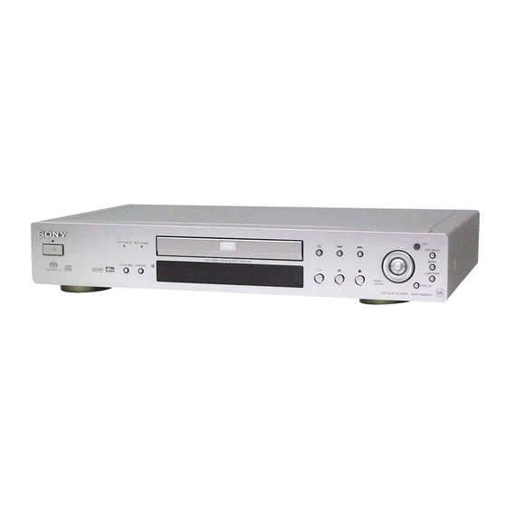
Photo: DVP-NS905V (Silver type)
SPECIFICATIONS
EXCEPT AEP, UK, Russian:
(Jack name: Jack type/Output level/Load
impedance)
LINE OUT (AUDIO) 1/2: Phono jack/
2 Vrms/10 kilohms
DIGITA L OUT (OPTICAL): Optical
output jack/–18 dBm (wave length:
660 nm)
DIGITA L OUT (COAXIAL): Phono jack/
0.5 Vp-p/75 ohms
5.1CH OUTPUT: Phono jack/2 Vrms/
10 kilohms
COMPONENT VIDEO OUT(Y, P
C
): Phono jack/Y: 1.0 Vp-p/P
R
C
: 0.7 Vp-p/75 ohms
R
LINE OUT (VIDEO) 1/2: Phono jack/
1.0 Vp-p/75 ohms
S VIDEO OUT 1/2: 4-pin mini DIN/Y:
1.0 Vp-p, C: 0.3 Vp-p (PAL), 0.286 Vp-p
(NTSC)/75 ohms
General
Power requirements:
110 V AC, 60 Hz
120 V AC, 60 Hz
220 V AC, 60 Hz
22
0–240 V AC, 50/60 Hz
110–240 V AC, 50/60 Hz
See page 1-1 for further information
Power consumption:
15 W
16 W
17
W
18 W
See page 1-1 for further information
DVP-NS705V/NS755V/
NS905V/NS915V
Saudi Arabia Model
New Zealand Model
Dimensions (approx.):
DVP-NS705V/NS755V:
430 × 74 × 257 mm (17 × 3 × 10
DVP-NS905V/NS915V:
430 × 77 × 257 mm (17 × 3
in.) (width/height/depth) incl. projecting
parts
Mass (approx.):
DVP-NS705V/NS755V:
2.6 kg (5
47
/
lb)
64
DVP-NS905V/NS915V:
2.8 kg (6
3
/
lb)
16
/C
, P
/
Operating temperature: 5 ° C to 35 ° C
B
B
R
/C
, P
/
(41
°
F to 95
°
F)
B
B
R
Operating humidity: 25 % to 80 %
Supplied accessories
Check that you have the following items:
• Audio/video cord (pinplug × 3 y pinplug
× 3) (1)
• Remote commander (remote) (1)
• Size AA (R6) batteries (2)
Specifications and design are subject to
change without notice.
E
S
NERGY
TAR
R
is a U.S. registered mark.
E
S
As an
NERGY
TAR
Corporation has determined that this product
E
S
meets the
NERGY
TAR
energy efficiency.
CD/DVD PLAYER
US Model
Canadian Model
DVP-NS755V
AEP Model
UK Model
DVP-NS705V/NS905V
E Model
DVP-NS915V
Russian Model
Middle East Model
Australian Model
DVP-NS905V
in.)
1
/
8
× 10
1
/
1
/
8
8
R
Partner, Sony
R
guidelines for
Advertisement
Table of Contents

Related Manuals for Sony DVP-NS705V


Summary of Contents for Sony DVP-NS705V
- Page 1 430 × 74 × 257 mm (17 × 3 × 10 in.) Signal format system: impedance) DVP-NS905V/NS915V: DVP-NS705V/NS905V: PAL (NTSC) LINE OUT (AUDIO) 1/2: Phono jack/ 430 × 77 × 257 mm (17 × 3 × 10 DVP-NS755V: NTSC 2 Vrms/10 kilohms in.) (width/height/depth) incl.
- Page 2 OPERATION. REPLACE THESE COMPONENTS WITH DE FONCTIONNEMENT. NE REMPLACER CES COM- SONY PARTS WHOSE PART NUMBERS APPEAR AS POSANTS QUE PAR DES PIÈCES SONY DONT LES SHOWN IN THIS MANUAL OR IN SUPPLEMENTS PUB- NUMÉROS SONT DONNÉS DANS CE MANUEL OU LISHED BY SONY.
-
Page 3: Table Of Contents
TABLE OF CONTENTS Section Title Page Section Title Page Service Note ................4 LE-34 (LED) Printed Wiring Board and Schematic Diagram ..........4-33 GENERAL AV-64 Printed Wiring Board .......... 4-35 AV-64 (VIDEO BUFFER) Schematic Diagram ....4-39 AV-64 (AUDIO AMP) Schematic Diagram ....4-41 Precautions .............. -
Page 4: Service Note
SERVICE NOTE 1. DISASSEMBLY • This set can be disassembled in the order shown below. Case (Page 2-1) Tray Cover Ass’y Power Block (Page 2-1) (Page 2-1) Mechanism Deck Front Panel Block (Page 2-2) Ass’y (Page 2-1) Optical Pick-Up AV-64 Board IF-94 Board (Page 2-3) (Page 2-2) - Page 5 2. DISC REMOVAL PROCEDURE 1) Remove the case from the set. (Refer to 2-1) 2) Remove the MB-105 board from the set. (Refer to 2-4) (at POWER OFF) 3) Set the MB-105 board as shown in Fig. 2. 1) Insert a tapering driver into the aperture of the unit bottom, and move the lever of chuck cam in the direction of the arrow 6 CK-122 board A.
- Page 6 5) Set the four flexible flat cables as shown in Fig. 4. 2 Flexible flat cable (FFC 9P: CN204) 3 Flexible flat cable 1 Flexible flat cable (FFC 5P: CN201) (FFC 26P: CN203) 4 Connector (CN112) 5 Connector (CN112) 7 Connector 6 Connector (CN202) (CN112)
-
Page 7: General
Sony dealer. shock. • Do not install the player in an inclined position. It is designed to be operated in a horizontal position only. -
Page 8: Index To Parts And Controls
Front panel display Index to Parts and Controls When playing back a DVD VIDEO/DVD-RW For more information, refer to the pages indicated in parentheses. Playing status Lights up when you can change the angle (60) Front panel Disc type Current audio signal (56) Playing time (52) DVP-NS755V Current play... -
Page 9: Simple Start Guide
List of Control Menu Items Guide to the Control Menu Display Item Item Name, Function, Relevant Disc Type TITLE (page 48)/SCENE (page 48)/TRACK (page 48) Use the Control Menu to select a function and to view related information. Press DISPLAY Selects the title, scene, or track to be played. -
Page 10: Hookups
z Hints Step 3: TV Hookups • To check the current setting of the player’s color system, press "/1. The power indicator lights up in green. If “NTSC” appears on the front panel display, the color system of the player is set to Connect the supplied audio/video cord and the power cord in the order (1~3) shown below. - Page 11 In the case of progressive scan picture problems, it is recommended that you switch the connection to the standard definition output. If there are questions regarding your Sony TV set’s compatibility with this DVD player, please contact our customer service center.
- Page 12 Connecting to a stereo amplifier (receiver) and 2 speakers/Connecting to Connecting to an AV amplifier (receiver) having a Dolby Surround (Pro an MD deck or DAT deck Logic) decoder and 3 to 6 speakers If the stereo amplifier (receiver) has audio input jacks L and R only, use .
- Page 13 Press ENTER. Press ENTER. Step 3: Connecting the Power Cord The Setup Display for selecting the The Setup Display for selecting the type aspect ratio of the TV to be connected of jack used to connect your amplifier appears. (receiver) appears. Plug the player and TV power cords into an AC outlet.
-
Page 14: Playing Discs
◆ When using an amplifier (receiver) Additional operations Locking the disc tray (Child Turn on the amplifier (receiver) and Lock) select the appropriate channel so that you Playing Discs can hear sound from the player. You can lock the disc tray to prevent children Playing Discs from opening it. - Page 15 Notes Resuming Playback From Using the DVD’s Menu Selecting “ORIGINAL” or • “MULTI-DISC RESUME” in “CUSTOM the Point Where You “PLAY LIST” on a DVD- SETUP” must be set to “ON” (default) for this function to work (page 78). Stopped the Disc RW Disc (Multi-disc •...
- Page 16 To return to the menu See the instructions of the CD-R/RW device Playing an MP3 Audio 1 ( 3 0 ) Press O RETURN. or recording software (not supplied) for details on the recording format. Track R O C K B E S T H I T z Hint K A R A O K E To play without using PBC, press ./>...
-
Page 17: Searching For A Scene
◆ When playing a VIDEO CD, Super To change or cancel a program Press SHUFFLE during playback. Playing repeatedly (Repeat Play) Audio CD, or CD The following display appears. Follow steps 1 through 3 of “Creating • DISC: repeats all of the tracks. your own program (Program Play).”... -
Page 18: Viewing Information About The Disc
Press ENTER. Dividing a scene into 9 sections Note Searching by Scene (STROBE PLAYBACK) You cannot search for a still picture on a DVD-RW in VR mode. (PICTURE NAVIGATION) To return to normal play You can display 9 consecutive moving Press O RETURN. -
Page 19: Sound Adjustments
To turn off the Control Menu Checking the play information of Checking the Play Press DISPLAY repeatedly until the Control a DATA CD Menu is turned off. Information By pressing TIME/TEXT while playing MP3 Display of each item audio tracks on a DATA CD, you can display By pressing DISPLAY repeatedly, you can You can check information such as the bit the audio bit rate (the amount of data per... -
Page 20: Enjoying Movies
◆TVS NIGHT ◆NORMAL SURROUND To cancel the setting SURROUND Mode Large sounds, such as explosions, are Software with 2 channel audio signals is Select “OFF” in step 2. suppressed, but the quieter sounds are decoded with the Dolby Surround (Pro Logic) Settings For 2 speaker setups unaffected. - Page 21 Press ENTER. Note Adjusting the Picture Adjusting the Playback The disc plays with the setting you Depending on the DVD VIDEO, you may not be Quality selected. Picture able to change the subtitles even if multilingual (BNR) (CUSTOM PICTURE MODE) subtitles are recorded on it.
-
Page 22: Using Various Additional Functions
To turn off the Custom Parental Control Press X/x to select function Using Various Additional (PARENTAL CONTROL), then press Functions ENTER. Follow steps 1 through 3 of “Custom Number The options for “PARENTAL Parental Control.” Locking Discs buttons CONTROL” appear. (CUSTOM Press X/x to select “OFF t,”... - Page 23 Switches to or from the wide The default setting of the Sound Feedback control your TV with the supplied remote. NS755V: mode of a Sony wide TV function is set to off. If you connect the player to an AV amplifier WIDE MODE...
-
Page 24: Settings And Adjustments
The options for “SETUP” appear. SCREEN SETUP Setting the Display or 4:3 LETTER BOX TV TYPE: ( 47 ) STOP Settings and Adjustments 4:3 LETTER BOX SCREEN SAVER: DVD VIDEO Sound Track Language BACKGROUND: 4:3 PAN SCAN COMPONENT OUT: 16:9 Using the Setup Display MODE: AUTO... - Page 25 ◆ PAUSE MODE (DVD VIDEO/DVD-RW Notes Custom Settings only) Settings for the Sound (CUSTOM • When you set the item to “AUTO,” the language Selects the picture in pause mode. SETUP) may change. The “TRACK SELECTION” setting (AUDIO SETUP) AUTO The picture, including subjects has higher priority than the “AUDIO”...
-
Page 26: Additional Information
“BALANCE” or “LEVEL” and adjust the DVD. Varies the level of each speaker. Be sure to Sony dealer. value of “BALANCE” using C/c and set “TEST TONE” to “ON” for easy Sound “LEVEL” using X/x. - Page 27 “.MP3.” display. be changed. , The data is not formatted in MP3 even , Contact your Sony dealer or local , Try using the DVD’s menu instead of the though it has the extension “.MP3.” authorized Sony service facility.
-
Page 28: Language Code List
Language Code List HD (high density) layer For details, see pages 55, 60, 74. • Super Audio CD (dual layer disc) The language spellings conform to the ISO 639: 1988 (E/F) standard. This disc consists of dual HD layers and is Code Language Code Language Code Language... -
Page 29: Disassembly
DVP-NS705V/NS755V/NS905V/NS915V SECTION 2 DISASSEMBLY Note: Follow the disassembly procedure in the numerical order given. 2-1. CASE REMOVAL 2-3. FRONT PANEL BLOCK ASS’Y REMOVAL 4 Case 1 Flexible board 3 Three screws (CN406) 5 Two claws (B3) 1 Tapping screw 4 Claw... -
Page 30: Mechanism Deck Removal
2-5. MECHANISM DECK REMOVAL 2-7. MB-105 BOARD REMOVAL 1 Flexible flat cable 2 Three screws (FAE-009: CN601) (B3) 4 Mechanism deck 2 Five screws 1 Two flexible flat cables 3 MB-105 board (B3) (FMO-001: CN203, FMO-002: CN204) 1 Flexible flat cable (FMM-035: CN201) 3 Two claws 2-6. -
Page 31: Board Removal
2-9. IF-94 BOARD REMOVAL 2 Two screws (B3) 3 FP support 5 Two screws (B3) 4 Connector (CN102) 6 Screw (B3) 1 Connector (CN201) 7 IF-94 board 2-10. OPTICAL PICK-UP REMOVAL 2 Insulator 2 Insulator 1 Insulator screw 2 Insulator 1 Insulator screw 1 Insulator screw... -
Page 32: Internal Views
2-11. INTERNAL VIEWS DC motor (loading) not supplied DC motor (loading) not supplied Optical pick-up (KHM-270AAA) A-6062-709-A... -
Page 33: Circuit Boards Location
2-12. CIRCUIT BOARDS LOCATION Power Block (ETXNY393N2F (NS705V/NS905V/NS915V: HK, SP, MY, TH, PH, IA, VTM, KR)) (HS12S1U (NS755V/NS915V: TW)) (HS12S1F (NS915V: LA)) ER-19 (SWITCHING REGULATOR) (NS705V/NS905V: AEP, UK, RUS) (EURO AV) AV-64 (AUDIO/VIDEO OUT) LE-34 (LED) MS-81 (LOADING) MB-105 (SIGNAL PROCESS, SERVO) IF-94 (INTERFACE CONTROL) 2-5 E... -
Page 34: Block Diagrams
DVP-NS705V/NS755V/NS905V/NS915V SECTION 3 BLOCK DIAGRAMS 3-1. OVERALL BLOCK DIAGRAM AV-64 BOARD (SEE PAGE 4-39 to 4-44) EXCEPT NS705V/NS905V :AEP, UK, RUS J103 MB-105 BOARD NS755V/NS915V (SEE PAGE 4-11 to 4-32) Y, Cb, Cr COMPONENT VIDEO OUT IC602 IC103 I/P CONVERTER... -
Page 35: Rf/Servo Block Diagram
DVP-NS705V/NS755V/NS905V/NS915V 3-2. RF/SERVO BLOCK DIAGRAM IC201 tl (DVD play) IC201 tl (CD play) IC201 2 (DVD play) IC201 2 (CD play) IC201 rs (DVD play) IC201 rs (CD play) 500 mV/DIV 50 ns/DIV 500 mV/DIV 200 ns/DIV 200 mV/DIV 50 ns/DIV... -
Page 36: Signal Processor Block Diagram
DVP-NS705V/NS755V/NS905V/NS915V 3-3. SIGNAL PROCESSOR BLOCK DIAGRAM MB-105 BOARD (2/5) (SEE PAGE 4-13 to 4-16) PCLK IC406 SDI 0 – 7 SDI 0 – 7 64M SDRAM IC303 XSRQ XSHD 16M DRAM SDCK AUDI0 1 XSAK (SEE PAGE 3-13) SDEF COLRCK/TDOKT TDOSA IC301 <zzz (DVD play) -
Page 37: System Control Block Diagram
DVP-NS705V/NS755V/NS905V/NS915V 3-4. SYSTEM CONTROL BLOCK DIAGRAM MB-105 BOARD (3/5) (SEE PAGE 4-19, 22) IC106 IC107 32M FLASH 1 – 5 18 – 21 HA 0 – 21 HA 0 – 21 HA 1 – 16 A 0 – 15 24 – 27 42 – 44 7 –... -
Page 38: Video (1) Block Diagram
DVP-NS705V/NS755V/NS905V/NS915V 3-5. VIDEO (1) BLOCK DIAGRAM MB-105 BOARD (4/5) NS705V (SEE PAGE 4-23, 25) COMPOUT YOUT COUT EXCEPT NS705V SIGNAL PROCESSOR (SEE PAGE 3-6) CR/B NS755V/NS915V CB/R IC602 <z/c Y_BUFF_CXD NS705V/NS905V:AEP, UK, RUS CN601 RGBSEL RGBSEL 1.6 Vp-p (66 MHz) -
Page 39: Video (2) Block Diagram
DVP-NS705V/NS755V/NS905V/NS915V 3-6. VIDEO (2) BLOCK DIAGRAM IC103 wa : AEP, UK, RUS ed : EXCEPT • Abbreviation AV-64 BOARD (1/2) * IC103 36 pin : EXCEPT AEP, UK, RUS EXCEPT AEP, UK, RUS J102 (1/2) AEP, UK, RUS (SEE PAGE 4-39) -
Page 40: Audio (1) Block Diagram
DVP-NS705V/NS755V/NS905V/NS915V 3-7. AUDIO (1) BLOCK DIAGRAM MB-105 BOARD (5/5) (SEE PAGE 4-27, 29, 31) CN501 (1/3) CDDOUT DSP1DII DSP2DO IC501 SPDIF 32 DSP2DII AUDIO DSP CN602 ACH12 160 DSP1CH12I (2/3) IC504 56 DSP2CH12I DSP2CH78O SDTI/DSDL AOUTL+ ALT+ ACH34 159 DSP1CH34I IC501 yl, <zvm... -
Page 41: Audio (2) Block Diagram
DVP-NS705V/NS755V/NS905V/NS915V 3-8. AUDIO (2) BLOCK DIAGRAM AV-64 BOARD (2/2) (SEE PAGE 4-41, 43) IC301 1 D IN OPTICAL DIGITAL CN201 (2/2) J301 Q301 SPDIF BUFFER COAXIAL IC303 LINE OUT AUDIO AMP J102 (2/2) CN301 (2/3) ALT+ ALT– – Q306 AUDIO 1... -
Page 42: Interface Control Block Diagram
DVP-NS705V/NS755V/NS905V/NS915V 3-9. INTERFACE CONTROL BLOCK DIAGRAM IF-94 BOARD (SEE PAGE 4-49) CN403 BZ401 BUZZER SYSTEM CONTROL XIFCS XIFCS (SEE PAGE 3-8) IFBSY IFBSY BUSY POWER 1 POWER (SEE PAGE 3-20) S411 XFRRST SURROUND XFRRST /FRRST POWER S410 PICTURE MODE CN402... -
Page 43: Power (1) Block Diagram
DVP-NS705V/NS755V/NS905V/NS915V 3-10. POWER (1) BLOCK DIAGRAM IF-94 BOARD (SEE PAGE 4-49) POWER SUPPLY BLOCK (ETXNY393N2F) (NS705V/NS905V/NS915V : HK, SP, KR) T101 CN401 (SEE PAGE 4-57) CN201 POWER INTERFACE CONTROL Q301 L301 D301 POWER (SEE PAGE 3-18) SW+11V • CN402 PS402... -
Page 44: Power (2) Block Diagram
DVP-NS705V/NS755V/NS905V/NS915V 3-11. POWER (2) BLOCK DIAGRAM AV-64 BOARD MB-105 BOARD (SEE PAGE 4-39 to 4-44) (SEE PAGE 4-25) CN301 CN302 CN602 CN601 CN901 • Abbreviation (1/2) L905 IC901 VIDEO+5V AI+5V VIDEO : Russian VIDEO–5V –5V BUFFER, VIDEO+11V +11V SELECT +11V... -
Page 45: Printed Wiring Boards And Schematic Diagrams
DVP-NS705V/NS755V/NS905V/NS915V SECTION 4 PRINTED WIRING BOARDS AND SCHEMATIC DIAGRAMS THIS NOTE IS COMMON FOR PRINTED WIRING For schematic diagram: • Caution when replacing chip parts. BOARDS AND SCHEMATIC DIAGRAMS. New parts must be attached after removal of chip. Be careful not to heat the minus side of tantalum capacitor, For printed wiring boards: because it is damaged by the heat. -
Page 46: Frame Schematic Diagram
DVP-NS705V/NS755V/NS905V/NS915V 4-1. FRAME SCHEMATIC DIAGRAM CN401 CN201 HS12S1U BOARD POWER POWER CN402 CN302 (NS755V/NS915V:TW) P-CONT SW-13V SW_-13V P-CONT EVER-13V EVER-13V AI+5V AI+5V HS12S1F BOARD M_GND M_GND AU+11V AU+11V HARNESS (NS915V:LA) M_GND (AF-123) D_GND_VIDEO M_GND SW+11V HARNESS SW+11V EVER+3.3V EVER+3.3V ETXNY393N2F... -
Page 47: Printed Wiring Boards And Schematic Diagrams
DVP-NS705V/NS755V/NS905V/NS915V 4-2. PRINTED WIRING BOARDS AND SCHEMATIC DIAGRAMS MS-81 (LOADING) PRINTED WIRING BOARD AND SCHEMATIC DIAGRAM – Ref. No.: MS-81 board; 1,000 series – There are a few cases that the part isn't mounted in this model is printed on this diagram. - Page 48 DVP-NS705V/NS755V/NS905V/NS915V There are a few cases that the part isn't mounted in this model is printed on this diagram. MB-105 (SIGNAL PROCESS, SERVO) PRINTED WIRING BOARD – Ref. No.: MB-105 board; 2,000 series – : Uses unleaded solder. MB-105 BOARD (SIDE A)
- Page 49 DVP-NS705V/NS755V/NS905V/NS915V MB-105 BOARD (SIDE B) MB-105 BOARD (SIDE B) D202 D501 E-10 D201 R212 C202 JL211 JL619 JL616 FL901 L202 R206 D502 E-10 JL621 JL613 FL201 JL204 IC901 C211 R211 R215 C209 D503 F-10 R248 R205 C207 L201 JL203 JL618...
-
Page 50: Rf Amp, Servo) Schematic Diagram
DVP-NS705V/NS755V/NS905V/NS915V The components identified by mark 0 or dotted Les composants identifiés par une marque 0 sont MB-105 (RF AMP, SERVO) SCHEMATIC DIAGRAM • See page 4-7 for printed wiring board. line with mark 0 are critical for safety. critiques pour la sécurité. Ne les remplacer que –... -
Page 51: Arp, Servo Dsp) Schematic Diagram
DVP-NS705V/NS755V/NS905V/NS915V MB-105 (ARP, SERVO DSP) SCHEMATIC DIAGRAM • See page 4-7 for printed wiring board. – Ref. No.: MB-105 board; 2,000 series – MB-105 BOARD (2/11) NO MARK:PB MODE MB-105 BOARD XRST (5/11) R360 C335 0.01u R337 MDPO MB-105 BOARD... -
Page 52: Av Decoder) Schematic Diagram
DVP-NS705V/NS755V/NS905V/NS915V MB-105 (AV DECODER) SCHEMATIC DIAGRAM • See page 4-7 for printed wiring board. – Ref. No.: MB-105 board; 2,000 series – MB-105 BOARD (3/11) NO MARK:PB MODE XWRH XAVDCS3 MB-105 BOARD (5/11) XAVDIT XAVDCS2 XWAIT 27MAVD MB-105 BOARD MB-105 BOARD... -
Page 53: Motor Drive) Schematic Diagram
DVP-NS705V/NS755V/NS905V/NS915V MB-105 (MOTOR DRIVE) SCHEMATIC DIAGRAM • See page 4-7 for printed wiring board. – Ref. No.: MB-105 board; 2,000 series – MB-105 BOARD (4/11) SIGNAL PATH SPINDLE SERVO(SPEED AND PHASE) NO MARK:PB MODE TRACKING SERVO DVD/CD CDV +3.3V SLED SERVO DVD/CD... -
Page 54: System Control) Schematic Diagram
DVP-NS705V/NS755V/NS905V/NS915V MB-105 (SYSTEM CONTROL) SCHEMATIC DIAGRAM • See page 4-7 for printed wiring board. – Ref. No.: MB-105 board; 2,000 series – MB-105 BOARD (5/11) XX MARK:NO MOUNT NO MARK:PB MODE +3.3V MB-105 BOARD (6/11) CN104 JL123 MB-105 BOARD (11/11) -
Page 55: Clock Generator) Schematic Diagram
DVP-NS705V/NS755V/NS905V/NS915V MB-105 (CLOCK GENERATOR) SCHEMATIC DIAGRAM • See page 4-7 for printed wiring board. – Ref. No.: MB-105 board; 2,000 series – • Waveforms 1 IC103 3, 4 MB-105 BOARD (6/11) NO MARK:PB MODE NS905V/NS915V IC102 IC102 TK11133CSCL-G +3.3V REG CONT 3.5 Vp-p (27 MHz) - Page 56 DVP-NS705V/NS755V/NS905V/NS915V MB-105 (I/P CONVERTER) SCHEMATIC DIAGRAM • See page 4-7 for printed wiring board. – Ref. No.: MB-105 board; 2,000 series – MB-105 BOARD (7/11) NO MARK:PB MODE NS755V/NS915V NS755V/NS915V R612 R613 MB-105 BOARD (5/11) R622 R626 R630 R634 R619...
-
Page 57: Video Encoder, Audio D/Aconverter) Schematic Diagram
DVP-NS705V/NS755V/NS905V/NS915V MB-105 (VIDEO ENCODER, AUDIO D/A CONVERTER) SCHEMATIC DIAGRAM • See page 4-7 for printed wiring board. – Ref. No.: MB-105 board; 2,000 series – SIGNAL PATH MB-105 BOARD (8/11) VIDEO SIGNAL AUDIO NO MARK:PB MODE SIGNAL CHROMA Y/CHROMA COMPOUT... -
Page 58: Mb-105 (Audio Dsp) Schematic Diagram
DVP-NS705V/NS755V/NS905V/NS915V MB-105 (AUDIO DSP) SCHEMATIC DIAGRAM • See page 4-7 for printed wiring board. – Ref. No.: MB-105 board; 2,000 series – • Waveforms 1 IC501 yl, <zvm MB-105 BOARD (9/11) NO MARK:DVD/CD PLAY D:DVD PLAY C:CD PLAY P:PAL DVD PLAY... -
Page 59: 2Ch/6Ch Dac) Schematic Diagram
DVP-NS705V/NS755V/NS905V/NS915V MB-105 (2ch/6ch DAC) SCHEMATIC DIAGRAM • See page 4-7 for printed wiring board. • Waveforms – Ref. No.: MB-105 board; 2,000 series – 1 IC504 4, IC502 qj MB-105 BOARD (10/11) DSCK MB-105 BOARD (11/11) DSADML NO MARK:DVD/CD PLAY... -
Page 60: Mb-105 (Sacd Decoder) Schematic Diagram
DVP-NS705V/NS755V/NS905V/NS915V MB-105 (SACD DECODER) SCHEMATIC DIAGRAM • See page 4-7 for printed wiring board. – Ref. No.: MB-105 board; 2,000 series – MB-105 BOARD (11/11) NO MARK:DVD/CD PLAY D:DVD PLAY C:CD PLAY *:IMPOSSIBLE TO MEASURE THE VOLTAGE AT THE MARKED POINTS. -
Page 61: Led) Printed Wiring Board And Schematic Diagram
DVP-NS705V/NS755V/NS905V/NS915V LE-34 (LED) PRINTED WIRING BOARD AND SCHEMATIC DIAGRAM – Ref. No.: LE-34 board; 1,000 series – There are a few cases that the part isn't mounted in this model is printed on this diagram. : Uses unleaded solder. LE-34 BOARD (SIDE B) - Page 62 DVP-NS705V/NS755V/NS905V/NS915V AV-64 (AUDIO/VIDEO OUT) PRINTED WIRING BOARD : Uses unleaded solder. – Ref. No.: AV-64 board; 1,000 series – There are a few cases that the part isn't mounted in this model is printed on this diagram. AV-64 BOARD (SIDE A)
- Page 63 DVP-NS705V/NS755V/NS905V/NS915V AEP, UK, RUS AUDIO VIDEO S VIDEO OUT AV-64 BOARD (SIDE B) 5.1CH OUTPUT EXCEPT AEP, UK, RUS FRONT REAR LINE OUT COMPONENT VIDEO OUT DIGITAL OUT CENTER AUDIO 1 VIDEO 1 COAXIAL OPTICAL S VIDEO OUT WOOFER AUDIO 2...
-
Page 64: Video Buffer) Schematic Diagram
DVP-NS705V/NS755V/NS905V/NS915V The components identified by mark 0 or dotted Les composants identifiés par une marque 0 sont AV-64 (VIDEO BUFFER) SCHEMATIC DIAGRAM • See page 4-35 for printed wiring board. line with mark 0 are critical for safety. critiques pour la sécurité. Ne les remplacer que –... -
Page 65: Audio Amp) Schematic Diagram
DVP-NS705V/NS755V/NS905V/NS915V AV-64 (AUDIO AMP) SCHEMATIC DIAGRAM • See page 4-35 for printed wiring board. – Ref. No.: AV-64 board; 1,000 series – AV-64 BOARD (2/3) EXCEPT NS905V:AEP,UK,RUS SIGNAL PATH NS705V/NS755V VIDEO SIGNAL R306 R311 NO MARK:PB MODE AUDIO R320 R322... -
Page 66: 5.1Ch Audio Amp) Schematic Diagram
DVP-NS705V/NS755V/NS905V/NS915V AV-64 (5.1CH AUDIO AMP) SCHEMATIC DIAGRAM • See page 4-35 for printed wiring board. – Ref. No.: AV-64 board; 1,000 series – EXCEPT NS905V:AEP,UK,RUS AV-64 BOARD (3/3) R206 R218 C226 R244 NS905V/NS915V C255 C260 2400 0.5% 3900p 0.5% 4700p 0.5%... -
Page 67: Printed Wiring Board
DVP-NS705V/NS755V/NS905V/NS915V IF-94 (INTERFACE CONTROL) PRINTED WIRING BOARD There are a few cases that the part isn't mounted in this model is printed on this diagram. – Ref. No.: IF-94 board; 1,000 series – : Uses unleaded solder. Power Block (ETXNY393N2F (NS705V/NS905V/NS915V: HK, SP, MY, TH, PH, IA, VTM, KR)) - Page 68 DVP-NS705V/NS755V/NS905V/NS915V IF-94 BOARD (SIDE B) IF-94 BOARD (SIDE B) CN403 I-20 CN405 I-22 JL411 JL413 JL415 JL417 CN406 H-23 CN402 CN407 D401 E-10 JL412 JL414 JL416 D402 E-10 D403 D404 D405 D406 C416 R401 D412 PS402 JL410 C409 C407 C408...
-
Page 69: If Con) Schematic Diagram
DVP-NS705V/NS755V/NS905V/NS915V IF-94 (IF CON) SCHEMATIC DIAGRAM – Ref. No.: IF-94 board; 1,000 series – IF-94 BOARD IC403 +1.8V REG NO MARK:DVD/CD PLAY IC403 *:IMPOSSIBLE TO MEASURE THE LMS8117ADTX-1.8/NOPB VOLTAGE AT THE MARKED POINTS. CN402 JL411 C403 SW-13V JL412 AI+5V JL413... - Page 70 DVP-NS705V/NS755V/NS905V/NS915V ER-19 (EURO AV) PRINTED WIRING BOARD : Uses unleaded solder. There are a few cases that the part isn't mounted in this model is printed on this diagram. – Ref. No.: ER-19 board; 1,000 series – – NS705V/NS905V: AEP, UK, RUS –...
- Page 71 DVP-NS705V/NS755V/NS905V/NS915V ER-19 (EAURO AV) SCHEMATIC DIAGRAM – Ref. No.: EAURO AV board; 4,000 series – – NS705V/NS905V: AEP, UK, RUS – ER-19 BOARD NO MARK:PB MODE NS705V R926 L905 22uH CN901 JL933 D906 CNJ902 JL917 1SR154-400TE-25 IC901 JL934 GND(E) C913...
-
Page 72: Etxny393N2F Printed Wiring Board
DVP-NS705V/NS755V/NS905V/NS915V ETXNY393N2F (SWITCHING REGULATOR) PRINTED WIRING BOARD There are a few cases that the part isn't mounted in this model is printed on this diagram. – Ref. No.: ETXNY393N2F board; 5,000 series – – NS705V/NS905V/NS915V: HK, SP, MY, TH, PH, IA, VTM, KR –... -
Page 73: Etxny393N2F (Switching Regulator) Schematic Diagram
DVP-NS705V/NS755V/NS905V/NS915V ETXNY393N2F (SWITCHING REGULATOR) SCHEMATIC DIAGRAM – Ref. No.: ETXNY393N2F board; 5,000 series – – NS705V/NS905V/NS915V: HK, SP, MY, TH, PH, IA, VTM, KR – ETXNY393N2F BOARD 2A 125V +11 (AUDIO) AC IN IF-94 BOARD CN401 (SEE PAGE 4-49) EVER+3.3V... - Page 74 DVP-NS705V/NS755V/NS905V/NS915V HS12S1U (SWITCHING REGULATOR) PRINTED WIRING BOARD There are a few cases that the part isn't mounted in this model is printed on this diagram. – Ref. No.: HS12S1U board; 5,000 series – – NS755V/NS915V: TW – : Uses unleaded solder.
- Page 75 DVP-NS705V/NS755V/NS905V/NS915V HS12S1U (SWITCHING REGULATOR) SCHEMATIC DIAGRAM • See page 4-37 for printed wiring board. The components identified by mark 0 or dotted Les composants identifiés par une marque 0 sont – Ref. No.: HS12S1U board; 5,000 series – line with mark 0 are critical for safety.
- Page 76 DVP-NS705V/NS755V/NS905V/NS915V HS12S1F (SWITCHING REGULATOR) PRINTED WIRING BOARD There are a few cases that the part isn't mounted in this model is printed on this diagram. – Ref. No.: HS12S1F board; 5,000 series – – NS915V: LA – : Uses unleaded solder.
- Page 77 DVP-NS705V/NS755V/NS905V/NS915V HS12S1F (SWITCHING REGULATOR) SCHEMATIC DIAGRAM • See page 4-37 for printed wiring board. The components identified by mark 0 or dotted Les composants identifiés par une marque 0 sont – Ref. No.: HS12S1F board; 5,000 series – line with mark 0 are critical for safety.
-
Page 78: Ic Pin Function Description
DVP-NS705V/NS755V/NS905V/NS915V SECTION 5 IC PIN FUNCTION DESCRIPTION... - Page 79 5-2 E...
-
Page 80: Test Mode
DVP-NS705V/NS755V/NS905V/NS915V SECTION 6 TEST MODE 6-1. GENERAL DESCRIPTION 6-3. SYSCON DIAGNOSIS The Test Mode allows you to make diagnosis and adjustment eas- The same contents as board detail check by serial interface can be ily using the remote commander and monitor TV. The instructions, checked from the remote commander. - Page 81 Submenu (2-6) Mount resistance confirmation check Error 22: region code discord. Selecting 2 and subsequent items calls the submenu screen of each Accordance between region codes, one is detected with item. model resistance and destination resistance, and the other Indication of “–” in the submenu means the check is not supported is detected with region resistance, is check.
- Page 82 5. Supply (5-5) ARP RAM Check (5-2) ARP Register Check Data write → read, and accord check Data write → read, and accord check Error 11: ARP RAM read data discord Error 08: ARP register write, and read data discord The program code data stored in ROM are copied to all Data 0x00 to 0xFF is written sequentially to the ARP TMAX areas of RAM (IC303) connected to the ARP (IC301)
- Page 83 7. Video Check Items List (7-2) Color Bar AVD color bar command write → Video OUT 2) Version Error: Not detected. (2-2) Revision The command is transferred to the AVD, and the color bar (2-3) ROM Check Sum signals are output from video terminals. (2-4) Model Type They are output from all video terminals (Composite, Y/C, (2-5) Region...
- Page 84 Error Codes List 00: Error not detected 01: RAM write/read data discord 03: EEPROM NG 04: Flash memory clear error 05: Flash memory write error 06: Flash memory read data discord 08: ARP register read data discord 09: ARP ←→ RAM data bus error 10: ARP ←→...
-
Page 85: Drive Auto Adjustment
1. DVD-SL (single layer) 6-4. DRIVE AUTO ADJUSTMENT [ENTER] Select , insert DVD single layer disc, and press key, and the adjustment will be made through the following steps, then On the Test Mode Menu screen, press key on the remote com- adjusted values will be written to the EEPROM. - Page 86 2. CD 3. DVD-DL (dual layer) [ENTER] [ENTER] Select , insert CD disc, and press key, and the adjust- Select , insert DVD dual layer disc, and press key, ment will be made through the following steps, then adjusted val- and the adjustment will be made through the following steps, then ues will be written to the EEPROM.
-
Page 87: Drive Manual Operation
0. Disc Check Memory 6-5. DRIVE MANUAL OPERATION Disc Check On the Test Mode Menu screen, select , and the manual opera- tion menu will be displayed. For the manual operation, each servo on/off control and adjustment can be executed manually. 1. - Page 88 Focus Search the focus and turn on the focus. Disc Type 1. Disc Type Auto Check Turn ON/OFF the tracking servo. 2. DVD SL 12cm 3. DVD DL 12cm 4. CD 12cm Sled Turn ON/OFF the sled servo. 5. SACD 12cm If PLL is not locked (or can not be 6.
- Page 89 5. Auto Adjustment ← Fj (L0 → L1) Focus jump reverse. (Trk/Sled Servo OFF) Auto Adjustment ↑ Lj (L1 → L0) Layer jump forward. 1. Auto TRK. Offset 2. Auto Focus Balance (Trk/Sled Servo ON) 3. Auto Focus Offset 4. Auto Focus Gain ↓...
-
Page 90: Mecha Aging
6-7. EMERGENCY HISTORY EEPROM DATA 3 -– DL -– CD LCD Analog FRSW xx xx ### EMG. History ### PLL Dac Gain xx xx Mirror Time xx xx Laser Hours xxhxxm xxhxxm THR A&L xx xx xx/xx xx : PREV Data 1. -
Page 91: Version Information
6-8. VERSION INFORMATION 6-10. IF CON SELF DIAGNOSTIC FUNCTION 1. IF-94 BOARD (IF CON) TEST MODE ### Version Infomation ### The front board test mode is the IF CON self diagnostic mode. IF con. Ver.x.xxx(xxxx) The IF CON can diagnose the functions of the front panel boards Group that the IF CON controls. - Page 92 2-2. Operation of Auto Self Check When the Self Check mode becomes active at the AC Power ON or by key input, the test display of the following steps (1) to (4) is repeated. (1) FLD and LED all ON (for 5 seconds) ;Digital GROUP TITLE TRACK CHAP INDEX ANGLE NTSC HOUR PROGRESSIVE MULTI...
- Page 93 2-3. Each Self Check Function Each Self Check function tests the FLD display, LED display, and key input. IC404: Pin No. (Signal) Input Voltage [V] Pin ed (CURSOR) Pin ef (O/C) Pin eg (PLAY) Pin eh (DISPLAY) Pin ej (POWER) 0 –...
- Page 94 Key code display (at input of key, Key code: 0Ah) ;Digital CHAP INDEX ANGLE NTSC HOUR GROUP TITLE TRACK PROGRESSIVE MULTI REPEAT MP 3 SHUFFLE At input of faulty voltage CHAP INDEX ANGLE NTSC HOUR ;Digital GROUP TITLE TRACK PROGRESSIVE MULTI REPEAT MP 3 SHUFFLE...
- Page 95 2-3-4. Communication Monitoring Display The communication state is monitored and displayed while the key name on the main unit and the remote commander is displayed. When the communication to the System Controller failed, VIDEO CD, DVD, and CD segments turn on. Communication error display (at no key input) GROUP TITLE TRACK CHAP INDEX ANGLE NTSC HOUR ;Digital...
- Page 96 2-3-6. FLD Grid Test Display and SHUTTLE Click Operation Test 2-3-6-1. Transition Keys in Self Check Mode • on the main unit and the remote commander ↑ • SHUTTLE on the remote commander during Grid Test display (This model does not provide JOG/SHUTTLE, and therefore use another DVD remote commander having the JOG/ SHUTTLE) 2-3-6-2.
- Page 97 GROUP TITLE TRACK CHAP INDEX ANGLE NTSC HOUR ;Digital PROGRESSIVE MULTI MP 3 REPEAT 1 SHUFFLE PGM A- ( 12G~1G ) ANODE CONNECTION ; Digital PROGRESSIVE MULTI MP 3 REPEAT SHUFFLE CHAP INDEX GROUP TITLE TRACK ANGLE NTSC HOUR 6-18...
-
Page 98: Troubleshooting
1-3. Clock signal check 6-11. TROUBLESHOOTING Measure the clock signal frequency at CPUCK (CL101) of 6-11-1. Cannot Enter Test Mode SYSCON (IC104) with an oscilloscope. You cannot enter the Test mode when either button has been pressed If the 8.25 MHz signal appears. t Check the machine ac- by any reason with the board assembled in the front panel. - Page 99 1-3-2. When the 33 MHz signal appears at CPUCK 3. If the message “SDSP No Ack” appears after the menu • WAIT signal check is displayed. 3-1. ARP & SERVO clock signal check Observe XWAIT (pin-yj) of SYSCON (IC104) with an os- cilloscope.
- Page 100 6-11-3. Drive Auto Adjustment stops due to error. 3-2. Check XFRRST (pin-9) at CN101 on the MB-105 The ARP & SERVO (IC301) analog circuit of MB-105 board is board. If it is fixed to “L”. t The signal line has defective solder- defective or RF-Amp (IC201) or M-Driver (IC202) peripheral cir- cuit is defective or optical pickup block is defective or flat cable ing, or is short-circuited with other signal lines, or parts are...
-
Page 101: Electrical Adjustment
DVP-NS705V/NS755V/NS905V/NS915V SECTION 7 ELECTRICAL ADJUSTMENT 7-1. POWER SUPPLY CHECK In making adjustment, refer to 7-6. Adjustment Related Parts Arrangement. 1. ETXNY393N2F Board: NS705V/NS905V/ NS915V: HK, SP, MY, Note: During diagnostic check, the characters and color bars can TH, PH, IA, VTM, KR be seen only with the NTSC monitor. -
Page 102: Adjustment Of Video System
7-2. ADJUSTMENT OF VIDEO SYSTEM 3. Checking S Video Output S-Y <Purpose> Check S-terminal video output. If it is incorrect, pictures will not 1. Video Level Adjustment (MB-105 BOARD) be displayed correctly in spite of connection to the TV with a S- <Purpose>... -
Page 103: Checking Component Video Output Y
5. Checking Component Video Output Y 7. Checking Component Video Output R-Y <Purpose> <Purpose> This checks component video output Y. If it is incorrect, correct This checks component video output R-Y. If it is incorrect, cor- brightness will not be attained when connected to, for instance, rect colors will not be displayed when connected to, for instance, projector. -
Page 104: Adjustment Related Parts Arrangement
7-3. ADJUSTMENT RELATED PARTS ARRANGEMENT MB-105 BOARD (SIDE A) IC403 RV401 (NS705V), RV601 (EXCEPT NS705V) RV602 (EXCEPT NS705V) VIDEO LEVEL ADJ COMP OUT RV601 RV401 RV602 ETXNY393N2F/HS12S1U/HS12S1F BOARD (SIDE A) CN201 7-6 E... -
Page 105: Repair Parts List
X-3952-392-1 COVER ASSY, TRAY (SILVER) 3-710-901-61 SCREW, TAPPING (SILVER) X-3952-397-1 COVER ASSY, TRAY (BLACK) 1-757-697-11 CABLE, FLEXIBLE FLAT (FMM-035) 3-066-225-01 SONY BADGE (5-A) (BLACK) 1-757-694-11 CABLE, FLEXIBLE FLAT (FMO-002) 3-066-225-11 SONY BADGE (5-A) (SILVER) 1-757-693-11 CABLE, FLEXIBLE FLAT (FMO-001) 3-073-096-01 LID, BATTERY COVER (for RMT-D146/D147) -
Page 106: Front Panel Assembly (Ns905V/Ns915V)
3-970-608-51 SUMITITE (B3), +BV X-3952-536-1 PANEL ASSY, FRONT (NS915V: EXCEPT LA) 1-757-697-11 CABLE, FLEXIBLE FLAT (FMM-035) 1-757-694-11 CABLE, FLEXIBLE FLAT (FMO-002) 4-942-568-41 EMBLEM (NO.5), SONY (NS905V: BLACK) 1-757-693-11 CABLE, FLEXIBLE FLAT (FMO-001) 4-942-568-51 EMBLEM (NO.5), SONY (NS915V) 4-942-568-61 EMBLEM (NO.5), SONY (NS905V: SILVER) -
Page 107: Chassis Assembly (Ns705V/Ns755V)
8-1-3. CHASSIS ASSEMBLY (NS705V/NS755V) NS-755V supplied NS-705V supplied not supplied not supplied NS-705V not supplied supplied mechanism deck not supplied not supplied not supplied The components identified by Les composants identifiés par une mark 0 or dotted line with marque 0 sont critiques pour la mark 0 are critical for safety. -
Page 108: Chassis Assembly (Ns905V/Ns915V)
8-1-4. CHASSIS ASSEMBLY (NS905V/NS915V) EXCEPT AEP, UK, RU supplied AEP, UK, RU supplied not supplied supplied AEP, UK, RU not supplied mechanism supplied deck supplied not supplied not supplied The components identified by Les composants identifiés par une mark 0 or dotted line with marque 0 sont critiques pour la mark 0 are critical for safety. -
Page 109: Mechanism Deck Assembly
8-1-5. MECHANISM DECK ASSEMBLY not supplied not supplied not supplied not supplied not supplied not supplied not supplied supplied supplied supplied not supplied not supplied The components identified by Les composants identifiés par une mark 0 or dotted line with marque 0 sont critiques pour la mark 0 are critical for safety. -
Page 110: Electrical Parts List
AV-64 8-2. ELECTRICAL PARTS LIST NOTE: The components identified by mark • Due to standardization, replacements in the • Items marked “*” are not stocked since they 0 or dotted line with mark 0 are parts list may be different from the parts speci- are seldom required for routine service. - Page 111 AV-64 Ref. No. Part No. Description Remark Ref. No. Part No. Description Remark C253 1-126-947-11 ELECT 47uF (NS705V/NS755V) C323 1-126-960-11 ELECT C254 1-115-416-11 CERAMIC CHIP 0.001uF (NS705V/NS905V: AEP, UK, RUS) C255 1-163-016-00 CERAMIC CHIP 0.0039uF 10% C333 1-163-016-00 CERAMIC CHIP 0.0039uF 10% (EXCEPT NS905V: AEP, UK, RUS) (EXCEPT NS905V: AEP, UK, RUS)
- Page 112 AV-64 Ref. No. Part No. Description Remark Ref. No. Part No. Description Remark IC203 8-759-684-22 IC BA15532F-E2 (NS905V/NS915V) R110 1-216-021-00 METAL CHIP 1/10W IC203 8-759-909-71 IC BA4558F-E2 (NS705V/NS755V) IC301 8-749-017-80 IC GP1FA551TZ (DIGITAL OUT OPTICAL) R111 1-216-021-00 METAL CHIP 1/10W (EXCEPT NS705V/NS905V: AEP, UK, RUS) IC302 8-759-052-52 IC NJM78M05DL1A-TE1...
- Page 113 AV-64 Ref. No. Part No. Description Remark Ref. No. Part No. Description Remark R232 1-216-660-11 METAL CHIP 2.4K 0.5% 1/10W R276 1-216-295-91 SHORT CHIP 0 (NS755V/NS915V) R233 1-216-660-11 METAL CHIP 2.4K 0.5% 1/10W R301 1-216-033-00 METAL CHIP 1/10W R234 1-216-660-11 METAL CHIP 2.4K 0.5% 1/10W...
- Page 114 AV-64 ER-19 Ref. No. Part No. Description Remark Ref. No. Part No. Description Remark R368 1-216-097-11 RES-CHIP 100K 1/10W D902 8-719-988-61 DIODE 1SS355TE-17 R370 1-469-324-21 FERRITE 0uH (NS705V) (NS905V: AEP, UK, RUS) D903 8-719-988-61 DIODE 1SS355TE-17 R370 1-216-295-91 SHORT CHIP 0 (EXCEPT NS705V) (NS905V: AEP, UK, RUS) D904...
- Page 115 ER-19 IF-94 Ref. No. Part No. Description Remark Ref. No. Part No. Description Remark < COIL > R923 1-216-041-00 METAL CHIP 1/10W (NS705V/NS905V: AEP, UK, RUS) L905 1-412-060-11 INDUCTOR 22uH R924 1-216-041-00 METAL CHIP 1/10W (NS705V/NS905V: AEP, UK, RUS) (NS705V/NS905V: AEP, UK, RUS) R925 1-216-295-91 SHORT CHIP 0 (NS705V)
- Page 116 IF-94 Ref. No. Part No. Description Remark Ref. No. Part No. Description Remark R408 1-216-073-91 RES-CHIP 1/10W C417 1-137-150-11 FILM 0.01uF 100V R409 1-216-073-91 RES-CHIP 1/10W C419 1-104-666-11 ELECT 220uF R411 1-216-025-11 RES-CHIP 1/10W C420 1-162-970-11 CERAMIC CHIP 0.01uF (EXCEPT NS705V) C421 1-162-964-11 CERAMIC CHIP 0.001uF...
- Page 117 IF-94 LE-34 MB-105 Ref. No. Part No. Description Remark Ref. No. Part No. Description Remark S402 1-771-349-21 SWITCH, KEYBOARD (O RETURN) C113 1-162-970-11 CERAMIC CHIP 0.01uF S403 1-771-349-21 SWITCH, KEYBOARD (MENU) S404 1-771-349-21 SWITCH, KEYBOARD (DISPLAY) C115 1-162-970-11 CERAMIC CHIP 0.01uF S405 1-771-349-21 SWITCH, KEYBOARD (x)
- Page 118 MB-105 Ref. No. Part No. Description Remark Ref. No. Part No. Description Remark C260 1-162-970-11 CERAMIC CHIP 0.01uF C411 1-162-970-11 CERAMIC CHIP 0.01uF C261 1-162-959-11 CERAMIC CHIP 330PF C413 1-162-970-11 CERAMIC CHIP 0.01uF C414 1-162-970-11 CERAMIC CHIP 0.01uF C262 1-107-826-11 CERAMIC CHIP 0.1uF C416 1-162-970-11 CERAMIC CHIP...
- Page 119 MB-105 Ref. No. Part No. Description Remark Ref. No. Part No. Description Remark C602 1-162-970-11 CERAMIC CHIP 0.01uF C634 1-127-715-91 CERAMIC CHIP 0.22uF (NS755V/NS915V) (EXCEPT NS705V) C603 1-162-964-11 CERAMIC CHIP 0.001uF C635 1-126-209-11 ELECT CHIP 100uF (NS755V/NS915V) (EXCEPT NS705V) C636 1-127-715-91 CERAMIC CHIP 0.22uF C604...
- Page 120 MB-105 Ref. No. Part No. Description Remark Ref. No. Part No. Description Remark FB107 1-469-324-21 FERRITE IC906 6-702-231-01 IC LMH6642MFX FB108 1-469-324-21 FERRITE FB109 1-469-324-21 FERRITE < COIL > FB110 1-469-324-21 FERRITE FB111 1-469-324-21 FERRITE L001 1-414-410-21 INDUCTOR 10uH L201 1-412-031-11 INDUCTOR CHIP 47uH FB112 1-469-784-11 FERRITE...
- Page 121 MB-105 Ref. No. Part No. Description Remark Ref. No. Part No. Description Remark R123 1-216-827-11 METAL CHIP 3.3K 1/10W R124 1-216-827-11 METAL CHIP 3.3K 1/10W R193 1-216-809-11 METAL CHIP 1/10W R125 1-216-833-11 METAL CHIP 1/10W R195 1-216-809-11 METAL CHIP 1/10W R196 1-216-809-11 METAL CHIP 1/10W...
- Page 122 MB-105 Ref. No. Part No. Description Remark Ref. No. Part No. Description Remark R434 1-216-797-11 METAL CHIP 1/10W R302 1-216-295-91 SHORT CHIP R310 1-216-821-11 METAL CHIP 1/10W R436 1-216-821-11 METAL CHIP 1/10W R311 1-216-809-11 METAL CHIP 1/10W (NS705V) R312 1-218-831-11 METAL CHIP 0.5% 1/10W R501...
- Page 123 MB-105 MS-81 Ref. No. Part No. Description Remark Ref. No. Part No. Description Remark R911 1-216-833-11 METAL CHIP 1/10W R628 1-216-801-11 METAL CHIP 1/10W R912 1-216-833-11 METAL CHIP 1/10W (NS755V/NS915V) R629 1-216-801-11 METAL CHIP 1/10W R913 1-216-803-11 METAL CHIP 1/10W (NS755V/NS915V) R914 1-216-833-11 METAL CHIP...
-
Page 124: Power Supply Block
POWER SUPPLY BLOCK POWER BLOCK (HS12S1U) POWER BLOCK (HS12S1F) Ref. No. Part No. Description Remark Ref. No. Part No. Description Remark 1-468-651-11 POWER SUPPLY BLOCK (ETXNY393N2F) 0 151 1-468-651-11 POWER SUPPLY BLOCK (ETXNY393N2F) (NS705V/NS905V/NS915V: EXCEPT HK, (NS905V/NS915V: HK, SP, MY, TH, SP, MY, TH, PH, IA, VTM, KR) PH, IA, VTM, KR) 0 151... - Page 125 DVP-NS705V/NS755V/NS905V/NS915V Sony Corporation 2002F0500-1 9-929-729-11 Home Video Campany © 2002. 6 – 180 – Published by Quality Assurance Dept.