Table of Contents
Advertisement
SERVICE MANUAL
Ver. 1.3 2008.08
• HCD-DZ30 is the amplifi er, DVD/CD and
tuner section in DAV-DZ30.
This system incorporates with Dolby* Digital and Dolby Pro Logic (II) adaptive
matrix surround decoder and the DTS** Digital Surround System.
* Manufactured under license from Dolby Laboratories.
"Dolby", "Pro Logic", and the double-D symbol are trademarks of Dolby
Laboratories.
** Manufactured under license from DTS, Inc.
"DTS" and "DTS Digital Surround" are registered trademarks of DTS, Inc.
Amplifi er section
Stereo mode (rated)
50 W + 50 W (at 3 ohms,
1 kHz, 1 % THD)
Surround mode (reference) RMS output power
FL/FR/C/SL/SR*: 67 watts
(per channel at 3 ohms,
1 kHz, 10 % THD)
Subwoofer*: 65 watts (at 3
ohms, 80 Hz, 10 % THD)
* Depending on the sound fi eld settings and the source,
there may be no sound output.
Inputs (Analog)
TV (AUDIO IN) (AEP, UK models)
Sensitivity: 450/250 mV
TV/VIDEO (AUDIO IN) (Except AEP, UK models)
Sensitivity: 450/250 mV
DVD system
Laser
Semiconductor laser
(DVD: λ = 650 nm)
(CD: λ = 790 nm)
Emission duration:
continuous
Signal format system
Mexican and Latin American model:
NTSC
Other models:
NTSC/PAL
Sony Corporation
9-887-992-04
2008H04-1
Audio&Video Business Group
©
2008.08
Published by Sony Techno Create Corporation
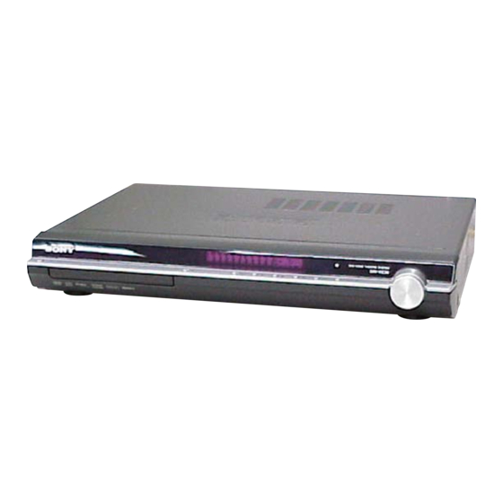
HCD-DZ30
Model Name Using Similar Mechanism
Mechanism Type
Optical Pick-up Name
SPECIFICATIONS
Tuner section
System
PLL quartz-locked digital
synthesizer
FM tuner section
Tuning range
North American models:
87.5 – 108.0 MHz
(100 kHz step)
Other models:
87.5 – 108.0 MHz
(50 kHz step)
Antenna (aerial)
FM wire antenna (aerial)
Antenna (aerial) terminals 75 ohms, unbalanced
Intermediate frequency
10.7 MHz
AM tuner section
Tuning range
North American, Mexican, and Latin American models:
530 – 1,710 kHz (with the
interval set at 10 kHz)
531 – 1,710 kHz (with the
interval set at 9 kHz)
European, Russian, and Middle Eastern models:
531 – 1,602 kHz (with the
interval set at 9 kHz)
Other models:
531 – 1,602 kHz (with the
interval set at 9 kHz)
530 – 1,610 kHz (with the
interval set at 10 kHz)
Antenna (aerial)
AM loop antenna (aerial)
Intermediate frequency
450 kHz
AEP Model
UK Model
E Model
HCD-DZ20
CDM85-DVBU102
KHM-313CAA
Video section
Outputs
AEP, UK models:
VIDEO: 1 Vp-p 75 ohms
R/G/B: 0.7 Vp-p 75 ohms
Except AEP, UK models:
VIDEO: 1 Vp-p 75 ohms
S VIDEO:
Y: 1 Vp-p 75 ohms
C: 0.286 Vp-p 75 ohms
COMPONENT:
Y: 1 Vp-p 75 ohms
P
/C
, P
/C
B
B
R
75 ohms
General
Power requirements
Mexican models:
120 V AC, 60 Hz
Venezuelan models:
120 V AC, 60 Hz
Argentine models:
220 – 240 V AC, 50/60 Hz
Latin American models:
110 – 240 V AC, 50/60 Hz
Other models:
220 – 240 V AC, 50/60 Hz
Power consumption
On: 80 W
Standby: 0.3 W (at the
Power Saving mode)
Dimensions (approx.)
430 mm × 67 mm ×
310 mm (w/h/d) incl.
projecting parts
Mass (approx.)
3.2 kg
Design and specifi cations are subject to change
without notice.
DVD RECEIVER
: 0.7 Vp-p
R
Advertisement
Table of Contents

Related Manuals for Sony HCD-DZ30


Summary of Contents for Sony HCD-DZ30
-
Page 1: Service Manual
SERVICE MANUAL AEP Model UK Model E Model Ver. 1.3 2008.08 • HCD-DZ30 is the amplifi er, DVD/CD and tuner section in DAV-DZ30. This system incorporates with Dolby* Digital and Dolby Pro Logic (II) adaptive Model Name Using Similar Mechanism HCD-DZ20 matrix surround decoder and the DTS** Digital Surround System. - Page 2 Strictly follow the instructions whenever the components are re- THE PARTS LIST ARE CRITICAL TO SAFE OPERATION. paired and/or replaced. REPLACE THESE COMPONENTS WITH SONY PARTS WHOSE PART NUMBERS APPEAR AS SHOWN IN THIS MANUAL OR IN SUPPLEMENTS PUBLISHED BY SONY.
-
Page 3: Table Of Contents
HCD-DZ30 TABLE OF CONTENTS SERVICING NOTES 6-4. Block Diagram –AMP Section– ........28 ..........6-5. Block Diagram –POWER Section– ........ 29 6-6. Printed Wiring Board –MAIN Board (Side A)– ..... 31 GENERAL ..............6-7. Printed Wiring Board –MAIN Board (Side B)– ..... 32 6-8. -
Page 4: Servicing Notes
HCD-DZ30 SECTION 1 SERVICING NOTES Note about CDs/DVDs NOTES ON HANDLING THE OPTICAL PICK-UP The system can play CD-ROMs/CD-Rs/CD-RWs recorded in the BLOCK OR BASE UNIT following formats: – audio CD format The laser diode in the optical pick-up block may suffer electrostat- –... - Page 5 TV screen. Although this is not a character service number (e.g., C 13 50) with a malfunction and for Sony service use only, combination of a letter and 4 digits appears on normal system operation will not be possible.
- Page 6 HCD-DZ30 Prevention of electric shock and damage to IC When disassembling the machine, be sure to discharge the charged electricity in the below point. Use a resistor of 800 ohms, 2 Watts for discharging. MAIN BOARD (SIDE A) 800 Ω/2W...
- Page 7 HCD-DZ30 MAIN board service position Please take the above-mentioned position in the repair of MAIN board. In that case, it is necessary the following extension cable during CN801 on FL board and CN509 on MAIN board. CN801 CN509 extension cable jig P/N: J-2501-231-A (pitch 1.00 mm/15p/300L)
-
Page 8: General
HCD-DZ30 SECTION 2 GENERAL This section is extracted from instruction manual. Front panel (on/standby) (18) (remote sensor) (8) VOLUME control (18) (open/close) (18) Disc tray (18) Disc operation (18) FUNCTION (18) Front panel display (78) ear panel AEP, UK MODEL... - Page 9 HCD-DZ30 ont panel display About the indications in the front panel display AEP, UK MODEL Lights up when the time information of Lights up when the child lock function a title or chapter appears in the front is set to on. (53) panel display.
-
Page 10: Remote Control
HCD-DZ30 Remote control ALPHABETICAL ORDER BUTTON DESCRIPTIONS A – O (on/standby) (13, 16, 18, P – Z 26, 48) ANGLE (36) PICTURE NAVI (26, 50) TV / (on/standby) (50) AUDIO (31) PRESET +/– (48) / / / / (13, 16, 19, 25,... -
Page 11: Disassembly
HCD-DZ30 SECTION 3 DISASSEMBLY • This set can be disassembled in the order shown below. 3-1. CASE (Page 12) 3-2. FRONT PANEL ASSY 3-5. MAIN BOARD 3-8. DVD MECHANISM DECK (Page 12) (Page 14) (Page 16) 3-3. FL BOARD 3-6. -
Page 12: Case
HCD-DZ30 Note: Follow the disassembly procedure in the numerical order shown below. 3-1. CASE case screw (CASE3 TP2) five screws (+BVTP 3 × 8) screw (CASE3 TP2) 3-2. FRONT PANEL ASSY The lever is moved in the direction of the arrow with the thin rod. -
Page 13: Fl Board
HCD-DZ30 3-3. FL BOARD wire (flat type) (15 core) (CN801) FL board two screws (+BVTP 2.6 (3CR)) shield (front) three screws (+BVTP 2.6 (3CR)) CN805 clamp screw (+BVTP 2.6 (3CR)) Route the wire (flat type) as shown below. clamp 3-4. -
Page 14: Main Board
HCD-DZ30 3-5. MAIN BOARD screw (+BVTP 3 × 12) two screws (+BV3 (3-CR)) Attaching the two radiation sheets on the IC MAIN board first, and then attach the heatsink (AMP). heatsink (AMP) heatsink (AMP) two radiation sheets radiation sheets IC on the... -
Page 15: Io Board (Aep, Uk)
HCD-DZ30 3-6. IO BOARD (AEP, UK) tuner (FM/AM) wire (flat type) (11 core) (CN101) wire (flat type) (13 core) (CN201) two screws (+BVTT 2.6 × 6) IO board two screws (+BVTP 3 × 8) wire (flat type) (17 core) (CN601) 3-7. -
Page 16: Dvd Mechanism Deck (Cdm85-Dvbu102)
HCD-DZ30 3-8. DVD MECHANISM DECK (CDM85-DVBU102) three screws (+BV3 (3-CR)) DVD mechanism deck (CDM85-DVBU102) The lever is moved in the direction of the arrow with the thin rod. CN1201 (6P) wire (flat type) (24 core) (CN1101) loading panel wire (flat type) (5 core) 3-9. -
Page 17: Belt, Ms-203 Board
HCD-DZ30 3-10. BELT, MS-203 BOARD chuck cam belt screw (M 1.7 × 2.5) two claws MS-203 board DC motor three claws... -
Page 18: Optical Pick-Up (Khm-313Caa)
HCD-DZ30 3-11. OPTICAL PICK-UP (KHM-313CAA) two claws chuck cam two claws base unit FFC holder two insulator screws two insulator screws two insulators optical pick-up (KHM-313CAA) two insulators two claws BU holder... -
Page 19: Test Mode
HCD-DZ30 SECTION 4 TEST MODE 3. Disc Tray Lock Note: Incorrect operations may be performed if the test mode is not The disc tray lock function for the antitheft of an demonstration entered properly. disc in the store is equipped. - Page 20 HCD-DZ30 (2) Select “2. Drive Manual Operation” by pressing the [2] button DVD SECTION on the remote commander. The screen will appear as shown. 7-1. GENERAL DESCRIPTION The IOP measurement allows you to make diagnosis and Drive Manual Operation adjustment simply by using the remote commander and monitor 1.
- Page 21 HCD-DZ30 7-4. EMERGENCY HISTORY 60: Focus on error 61: Seek fail error To check the emergency history, please follow the following 62: Read Q data/ID error procedure. 70: Lead in data read fail 71: TOC read time out (CD) (1) From the Top Menu of Remocon Diagnosis Menu, select “3.
- Page 22 HCD-DZ30 7-4-4. Return to the Top Menu of Remocon Diagnosis 10. PROTECTION FACTOR (SD DETECTION/ Menu DC DETECTION) IDENTIFICATION TEST MODE Press [0] button on the remote commander. When an error is detected, the FL tube alternately displays “PROTECTOR h PUSH POWER”.
-
Page 23: Electrical Adjustments
HCD-DZ30 SECTION 5 ELECTRICAL ADJUSTMENTS DVD SECTION When the optical pick-up assy is replaced, perform the “EXECUTING IOP MEASUREMENT”. EXECUTING IOP MEASUREMENT (See page 20) TUNER SECTION [FM Tune Level Check] generator OUT (75 Ω) Procedure: 1. Turn the power on. - Page 24 HCD-DZ30 MEMO...
-
Page 25: Diagrams
HCD-DZ30 SECTION 6 DIAGRAMS 6-1. BLOCK DIAGRAM – RF Section – DVDRFIP DVDA DVDB DETECTOR DVDC DVDD • Signal Path : CD PLAY : DVD PLAY OPTICAL PICK-UP IC1101 (1/3) BLOCK CD/DVD RF AMP, (KHM-313CAA) FOCUS/TRACKING ERROR AMP DVD SYSTEM PROCESSOR... -
Page 26: Block Diagram -Video Section
HCD-DZ30 6-2. BLOCK DIAGRAM – VIDEO Section – AEP, UK MODEL J203 CROUT R/C OUT CYOUT G OUT IC201 VIDEO AMP, 75Ω DRIVER CBOUT B OUT VOUT V/Y OUT EURO AV BLANK CYOUT OUTPUT CYOUT (TO TV) CBOUT CBOUT FUNCTION... -
Page 27: Block Diagram -Audio Section
HCD-DZ30 6-3. BLOCK DIAGRAM – AUDIO Section – IC2200 A/D CONVERTER DATA1 – DATA3, ACLK, 13 LIN DOUT ABCK, ALRCK ALRCK SECTION ABCK (Page 28) R-CH 14 RIN SCKI DATA1 LRCK DATA3 ALRCK ABCK ACLK ACLK 209 SPDATA/SMSDI ASDATA0 DATA2... -
Page 28: Block Diagram -Amp Section
HCD-DZ30 6-4. BLOCK DIAGRAM – AMP Section – IC3100 IC3010 SPEAKER POWER DRIVER SYSTEM PROCESSOR DATA1 - DATA3, ACLK, ABCK, ALRCK DATA1 AUDIO 31 DATA OUTR1 2 PWMBP OUTB FRONT SECTION ACLK (Page 27) 36 XFSIIN OUTR2 PWMAP OUTA ABCK... -
Page 29: Block Diagram -Power Section
HCD-DZ30 6-5. BLOCK DIAGRAM – POWER Section – T901 D901 TRANSFORMER(MAIN) AC IN D931 IC901 D905 +21.7V Q901 SWITCHING DC/DC VOLTAGE REGULATOR CONVERTER CONTROLLER IC931 T801 VOLTAGE DETECT PC901 TO VACUUM PHOTO FLUORESCENT RECT COUPLER DISPLAY D801,802 D804,805 Q943,947 PC903... - Page 30 HCD-DZ30 Ver. 1.3 THIS NOTE IS COMMON FOR PRINTED WIRING BOARDS AND SCHEMATIC DIAGRAMS. • Waveforms – MAIN Board – – IO Board – (In addition to this, the necessary note is printed in each block.) For Printed Wiring Boards.
-
Page 31: Printed Wiring Board -Main Board (Side A)
HCD-DZ30 Ver. 1.3 6-6. PRINTED WIRING BOARD – MAIN Board (Side A) – • See page 30 for Circuit Boards Location. • : Uses unleaded solder. MAIN BOARD (SIDE A) • Semiconductor Location Ref. No. Location D910 I-11 D914 G-11... -
Page 32: Printed Wiring Board -Main Board (Side B)
HCD-DZ30 Ver. 1.3 6-7. PRINTED WIRING BOARD – MAIN Board (Side B) – • See page 30 for Circuit Boards Location. • : Uses unleaded solder. SPEAKER CENTER WOOFER FRONT R FRONT L SUR R SUR L • Semiconductor MAIN BOARD... -
Page 33: Schematic Diagram -Main Board (1/8)
HCD-DZ30 6-8. SCHEMATIC DIAGRAM – MAIN Board (1/8) – • See page 30 for waveforms. • See page 49 for IC Pin Function Description of IC1101. MAIN BOARD (1/8) R1183 R1132 100k SW+5V C1150 MAIN BOARD R1136 C1135 C1137 C1139... -
Page 34: Schematic Diagram -Main Board (2/8)
HCD-DZ30 Ver. 1.3 6-9. SCHEMATIC DIAGRAM – MAIN Board (2/8) – • See page 46 for IC Block Diagrams. (CHASSIS) CN1301 MAIN BOARD JL1713 IC1104 (2/8) C1197 V-GND JL1711 64M SDRAM RA[4] RA[3] V-GND JL1709 RA[5] RA[2] RA[6] RA[1] V-GND... -
Page 35: Schematic Diagram -Main Board (3/8)
HCD-DZ30 Ver. 1.3 6-10. SCHEMATIC DIAGRAM – MAIN Board (3/8) – • See page 30 for waveform. • See page 54 for IC Pin Function Description of IC501. MAIN BOARD (3/8) D-GND M_ST M_ST R525 R524 DC_DETECT DC_DETECT OVERFLOW2 TP520... -
Page 36: Schematic Diagram -Main Board (4/8)
HCD-DZ30 6-11. SCHEMATIC DIAGRAM – MAIN Board (4/8) – • See page 46 for IC Block Diagram. MAIN BOARD (4/8) C3401 Q3551 2SC3052EF-T1-LEF PROTECT DETECT IC3400 IC3400 CXD9774M ICT360 12.0 POWER DRIVER GREG 12.0 R3554 C3555 PWM_BP GVDD 100k R3060... -
Page 37: Schematic Diagram -Main Board (5/8)
HCD-DZ30 6-12. SCHEMATIC DIAGRAM – MAIN Board (5/8) – • See page 46 for IC Block Diagram. (Page 36) MAIN BOARD (4/8) MAIN BOARD (5/8) C3251 IC3250 CXD9774M IC3250 12.0 GREG POWER DRIVER 12.0 PWM_BP GVDD L3252 NSP_MUTE 10uH PVSS... -
Page 38: Schematic Diagram -Main Board (6/8)
HCD-DZ30 6-13. SCHEMATIC DIAGRAM – MAIN Board (6/8) – • See page 30 for waveform. • See page 46 for IC Block Diagrams. (Page 37) MAIN BOARD (5/8) C3151 MAIN BOARD (6/8) IC3150 CXD9774M IC3150 12.0 GREG POWER DRIVER CL003... -
Page 39: Schematic Diagram -Main Board (7/8)
HCD-DZ30 6-14. SCHEMATIC DIAGRAM – MAIN Board (7/8) – MAIN BOARD (7/8) MAIN BOARD SW+5V (3/8) (Page 35) IOPMON R1223 R1231 100k R1225 R1234 0.5% 100k 0.5% 0.5% ICT550 R1232 R1221 FCS- R1233 C1209 R1230 FCS- 0.033 0.5% 0.5% 0.5% FCS+ 0.5%... -
Page 40: Schematic Diagram -Main Board (8/8)
HCD-DZ30 Ver. 1.3 6-15. SCHEMATIC DIAGRAM – MAIN Board (8/8) – • See page 47 for IC Block Diagram. (CHASSIS) (CHASSIS) MAIN BOARD (8/8) C963,964 C905 470p, 250V (EXCEPT E87,MX) C938 0.0033, 400V (EXCEPT E87,MX) 470p 0.0022, 250V (E87,MX) 0.01, 400V... -
Page 41: Printed Wiring Board -Ms-203 Board
HCD-DZ30 6-16. PRINTED WIRING BOARD – MS-203 Board – 6-17. SCHEMATIC DIAGRAM – MS-203 Board – • See page 30 for Circuit Boards Location. • : Uses unleaded solder. MS-203 BOARD CN001 S001 (CHUCK/TRAY DETECT) CN001 MAIN BOARD CN1202 M203... -
Page 42: Printed Wiring Board -Io Board
HCD-DZ30 Ver. 1.1 6-18. PRINTED WIRING BOARD – IO Board – • See page 30 for Circuit Boards Location. • : Uses unleaded solder. IO BOARD • Semiconductor Location Ref. No. Location EXCEPT AEP,UK MODEL D200 J201 D201 MONITOR OUT... -
Page 43: Schematic Diagram -Io Board
HCD-DZ30 Ver. 1.1 6-19. SCHEMATIC DIAGRAM – IO Board – • See page 30 for waveforms. • See page 47 for IC Block Diagram. AEP, UK MODEL EXCEPT AEP, UK MODEL TN901 TN901 COAXIAL COAXIAL TUNER TUNER FM75 FM75 EXCEPT AEP, UK MODEL... -
Page 44: Printed Wiring Boards -Key, Fl, P-Sw Board
HCD-DZ30 6-20. PRINTED WIRING BOARDS – KEY, FL, P-SW Board – • See page 30 for Circuit Boards Location. • : Uses unleaded solder. (Page 32) MAIN BOARD CN509 FL BOARD R805 IC801 R804 JW829 R801 CN801 D801 L801 JL002... -
Page 45: Schematic Diagram -Key, Fl, P-Sw Board
HCD-DZ30 6-21. SCHEMATIC DIAGRAM – KEY, FL, P-SW Board – • See page 48 for IC Block Diagram. R857 R856 R855 KEY BOARD 2.2K 2.2k S806 S805 S804 C853 CN809 100p P-SW BOARD S800 VOLUME R852 KEY0 R851 3.3k CN804... - Page 46 HCD-DZ30 • IC Block Diagrams IC2200 PCM1808PWR (MAIN Board (2/8)) IC3010 CDX9843AR (MAIN Board (6/8)) IC3020 CDX9843AR (MAIN Board (5/8)) IC3030 CDX9843AR (MAIN Board (4/8)) LRCK Serial Interface DOUT Mode/ Format Control OVF FLAG L Clock Serial Control Timing SCKI...
- Page 47 HCD-DZ30 Ver. 1.3 IC901 STR-F6168-LF1352 (EXCEPT E87, MX MODEL) (MAIN Board (8/8)) IC901 STR-F6138-LF1352 (E87, MX MODEL) (MAIN Board (8/8)) FB/OLP Reg2 Drain UVL0 Delay POWER ON=16V – MOS FET OFF=10.5V Delay Reg1 IOLP Latch Internal S/GND – Bias OCP1 Volp –...
- Page 48 HCD-DZ30 IC802 PT6315 (FL Board) Grid driver Multiplexed driver SEG19/GRID10 Command decoder LED1 SEG18/GRID11 LED2 Display memory LED3 SEG17/GRID12 24 bits x 12 words LED4 Timing generator key scan DOUT SEG16/KS16 Key data memory Serial SEG15/KS15 (2 x 16 bits)
- Page 49 HCD-DZ30 • IC Pin Function Description MAIN BOARD IC1101 CXD9849R (CD/DVD RF AMP, FOCUS/TRACKING ERROR AMP, DVD SYSTEM PROCESSOR, DIGITAL SERVO PROCESSOR) Pin No. Pin Name Description AGND — Ground terminal DVDA AC coupled input path A DVDB AC coupled input path B...
- Page 50 HCD-DZ30 Pin No. Pin Name Description 53 to 58 IOA 2 to 7 Address bus 2 to 7 output to PROM (IC1102) HIGHA0 Address bus 8 output to PROM (IC1102) 60, 61 IOA18, 19 Address bus 18, 19 output to PROM (IC1102) DVSS —...
- Page 51 HCD-DZ30 Pin No. Pin Name Description 128 to 133 RD 14 to 9 Data bus 14 to 9 from SD-RAM (IC1104) DVSS — Ground terminal Data bus 8 from SD-RAM (IC1104) GPI0 — Not used (Open) DQM1 DQM1 signal output to SD-RAM (IC1104)
- Page 52 HCD-DZ30 Pin No. Pin Name Description YUV1 Y signal output to VIDEO AMP (IC201) DAVDD — Power Supply (+3.3V) YUV2 CHROMA signal output to VIDEO AMP (IC201) DAVSS — Ground terminal YUV3 VIDEO signal output to VIDEO AMP (IC201) DAVDD —...
- Page 53 HCD-DZ30 Pin No. Pin Name Description RFGND — Ground terminal EQ offset loop capacitance (not used (Open)) EQ offset loop capacitance (not used (Open)) RF offset cancellation capacitor connecting RF offset cancellation capacitor connecting RFGC RF offset loop capacitor connecting for DVD-ROM...
- Page 54 HCD-DZ30 MAIN BOARD IC501 M30622MEP-B20FPU0 (SYSTEM CONTROLLER) Pin No. Pin Name Description DAMP_SCDT Digital amp (IC3010, 3020, 3030) data output DAMP_SHIFT Digital amp (IC3010, 3020, 3030) data output NO USE Not used (Open) SIRCS_IN Sircs input NO USE Not used (Open)
- Page 55 HCD-DZ30 Pin No. Pin Name Description FL_STB FL driver (IC802) chip select signal output DC_DETECT Speaker DC detect input NO USE Not used (Open) NO USE Not used (Open) NO USE Not used (Open) NO USE Not used (Open) —...
-
Page 56: Exploded Views
HCD-DZ30 Ver. 1.3 SECTION 7 EXPLODED VIEWS Note: • -XX and -X mean standardized parts, so • Abbreviation The components identifi ed by mark 0 they may have some difference from the : 240V AC area in E model or dotted line with mark 0 are critical for original one. -
Page 57: Front Panel Assy
HCD-DZ30 Ver. 1.1 7-2. FRONT PANEL ASSY not supplied not supplied (P-SW board) ND001 not supplied not supplied not supplied not supplied not supplied not supplied (KEY board) including S800 Ref. No. Part No. Description Remark Ref. No. Part No. -
Page 58: Dvd Mechanism Deck Section (Cdm85-Dvbu102)
HCD-DZ30 7-3. DVD MECHANISM DECK SECTION (CDM85-DVBU102) not supplied not supplied not supplied not supplied not supplied not supplied (MS-203 board) not supplied not supplied supplied Ref. No. Part No. Description Remark Ref. No. Part No. Description Remark A-6071-669-A LOADING ASSY (M) -
Page 59: Electrical Parts List
HCD-DZ30 Ver. 1.3 SECTION 8 ELECTRICAL PARTS LIST Note: • Due to standardization, replacements in • COILS When indicating parts by reference num- the parts list may be different from the uH: μH ber, please include the board name. parts specifi ed in the diagrams or the com- •... - Page 60 HCD-DZ30 Ver. 1.1 Ref. No. Part No. Description Remark Ref. No. Part No. Description Remark C228 1-126-916-11 ELECT 1000uF 6.3V < TERMINAL BOARD > (AEP,UK) C228 1-126-933-11 ELECT 100uF J201 1-694-920-11 TERMINAL BOARD (S TERMINAL+1P) (EXCEPT AEP,UK) (MONITOR OUT S VIDEO/VIDEO)
- Page 61 HCD-DZ30 Ver. 1.3 MAIN Ref. No. Part No. Description Remark Ref. No. Part No. Description Remark R249 1-216-821-11 METAL CHIP 1/10W C850 1-162-970-11 CERAMIC CHIP 0.01uF (AEP,UK) C852 1-162-927-11 CERAMIC CHIP 100PF R250 1-216-825-11 METAL CHIP 2.2K 1/10W C853 1-162-927-11...
- Page 62 HCD-DZ30 Ver. 1.3 MAIN Ref. No. Part No. Description Remark Ref. No. Part No. Description Remark C598 1-127-573-11 CERAMIC CHIP 1uF C1102 1-165-908-11 CERAMIC CHIP 1uF C599 1-126-947-11 ELECT 47uF C1105 1-126-947-11 ELECT 47uF 0 C901 1-165-529-11 MYLAR 0.22uF 275V...
- Page 63 HCD-DZ30 Ver. 1.1 MAIN Ref. No. Part No. Description Remark Ref. No. Part No. Description Remark C1182 1-127-715-11 CERAMIC CHIP 0.22uF C3039 1-164-156-11 CERAMIC CHIP 0.1uF C1184 1-162-970-11 CERAMIC CHIP 0.01uF C3040 1-164-156-11 CERAMIC CHIP 0.1uF C1186 1-127-715-11 CERAMIC CHIP 0.22uF...
- Page 64 HCD-DZ30 Ver. 1.3 MAIN Ref. No. Part No. Description Remark Ref. No. Part No. Description Remark C3216 1-126-942-61 ELECT 1000uF CN1101 1-815-763-32 CONNECTOR, FFC/FPC 24P C3221 1-164-505-11 CERAMIC CHIP 2.2uF * CN1105 1-564-708-11 PIN, CONNECTOR (SMALL TYPE) 6P C3222 1-162-970-11 CERAMIC CHIP 0.01uF...
- Page 65 HCD-DZ30 Ver. 1.3 MAIN Ref. No. Part No. Description Remark Ref. No. Part No. Description Remark IC943 6-705-308-01 IC SI-3010KM-TL L3053 1-414-754-11 INDUCTOR 10uH IC951 6-707-743-01 IC TA76L431S(TPE6,Q) L3054 1-412-939-11 INDUCTOR IC1101 6-707-535-01 IC CXD9849R L3111 1-456-680-11 COIL, CHOKE 10uH...
- Page 66 HCD-DZ30 Ver. 1.3 MAIN Ref. No. Part No. Description Remark Ref. No. Part No. Description Remark R511 1-216-829-11 METAL CHIP 4.7K 1/10W 0 R901 1-219-759-11 METAL 1/2W (AEP) 0 R903 1-215-926-00 METAL OXIDE R511 1-216-831-11 METAL CHIP 6.8K 1/10W (E87,MX)
- Page 67 HCD-DZ30 Ver. 1.1 MAIN Ref. No. Part No. Description Remark Ref. No. Part No. Description Remark R970 1-216-864-11 SHORT CHIP R1216 1-216-834-11 METAL CHIP 1/10W R974 1-216-827-11 METAL CHIP 3.3K 1/10W R1219 1-216-838-11 METAL CHIP 1/10W R1101 1-216-809-11 METAL CHIP...
- Page 68 HCD-DZ30 Ver. 1.1 MAIN Ref. No. Part No. Description Remark Ref. No. Part No. Description Remark R3014 1-216-809-11 METAL CHIP 1/10W R3151 1-216-809-11 METAL CHIP 1/10W R3015 1-216-809-11 METAL CHIP 1/10W R3152 1-216-809-11 METAL CHIP 1/10W R3017 1-216-809-11 METAL CHIP...
- Page 69 HCD-DZ30 Ver. 1.3 MAIN MS-203 P-SW Ref. No. Part No. Description Remark Ref. No. Part No. Description Remark R3409 1-216-864-11 SHORT CHIP P-SW BOARD R3411 1-220-942-11 METAL CHIP 1/4W *********** R3412 1-220-942-11 METAL CHIP 1/4W R3421 1-216-833-11 METAL CHIP 1/10W <...
-
Page 70: Revision History
HCD-DZ30 REVISION HISTORY Checking the version allows you to jump to the revised page. Also, clicking the version at the top of the revised page allows you to jump to the next revised page. Ver. Date Description of Revision 2008.02 2008.04...