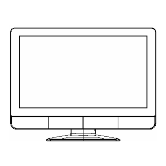
Vizio VX32L Service Manual
Hide thumbs
Also See for VX32L:
- User manual (67 pages) ,
- Service manual (42 pages) ,
- Quick start manual (2 pages)

Related Manuals for Vizio VX32L


Summary of Contents for Vizio VX32L
-
Page 1: Service Manual
Service Manual Model #: VIZIO VX32L HDTV V, Inc 320A Kalmus Drive Costa Mesa, CA 92626 TEL : +714-668-0588 FAX :+714-668-9099 Top Confidential... -
Page 2: Table Of Contents
8. Waveforms 9. Trouble Shooting 10. Block Diagram 10-1 11. Spare parts list 11-1 12. Complete Parts List 12-1 Appendix 1. Main Board Circuit Diagram 2. Main Board PCB Layout 3. Assembly Explosion Drawing Block Diagram VIZIO VX32L HDTV Service Manual... - Page 3 Use a power cable that is properly grounded. Always use the AC cords as follows – USA (UL); Canada (CSA); Germany (VDE); Switzerland (SEV); Britain (BASEC/BS); Japan (Electric Appliance Control Act); or an AC cord that meets the local safety standards. VIZIO VX32L HDTV Service Manual...
-
Page 4: Features
Chapter 1 Features 1. Built in TV channel selector for TV viewing 2. Simulatnueous display of PC and TV images 3. Connectable to PC’s analog RGB port 4. Built in S-video, HDTV, composite video, HDMI and TV out 5. Built in auto adjust function for automatic adjument of screen display 6. - Page 5 Chapter 2 Specification 1. LCD CHARACTERISTICS LC320W01 Item Specification 31.51(800.4mm) inch diagonal Active Screen Size 760.0mm(H) x 450.0mm(V) x 48.0mm(D) (Typ.) Outline Dimension 0.17025mm x 0.51075mm xRGB Pixel Pitch Pixel Format 1366 (R,G,Bx3) x 768 Display Color 16.7 M (8-bit + FRC for R,G,B) Luminance, White 500 cd/m (Typ)
- Page 6 5. POWER SUPPLY Power Consumption: 180W MAX Power OFF: to less than 3W MAX 6.Speaker Output 10W (max) X2 7. ENVIRONMENT 7-1. Operating Temperature: 5c~35c (Ambient) 7-2. Operating Humidity: Ta= 35 °C, 90%RH (Non-condensing) 7-3. Operating Altitude: 0 - 14,000 feet (Non-Operating) 8.
- Page 7 (5) Acetic acid type and chlorine type materials for the cover case are not desirable because the former generates corrosive gas of attacking the polarizer at high temperature and the latter causes circuit break by electro-chemical reaction. (6) Do not touch, push or rub the exposed polarizes with glass, tweezers or anything harder than HB pencil lead.
- Page 8 9-3. HANDLING PRECAUTIONS FOR PROTECTION (1) The protection film is attached to the bezel with a small masking tape. When the protection film is peeled off, static electricity is generated between the film and polarizer. This should be peeled off slowly and carefully by people who are electrically grounded and with well ion-blown equipment or in such a condition, etc.
- Page 9 Chapter 3 On Screen Display Main unit button Power MENU CH ▲ CH ▼ VOL + VOL - Input TV Source A. PICTURE: a. PICTURE MODE (CUSTOM/ STANDARD / MOVIE / GAME) b. BACKLIGHT (0~100) c. BRIGHTNESS (0~100) d. CONTRAST (0~100) e.
- Page 10 B. AUDIO: a. VOLUME (0~100) b. BASS (0~100) c. TREBLE (0~100) d. BALANCE (-50~50) e. SURROUND (ON/OFF) SPEAKERS (ON/OFF) C. TV: a. TUNER MODE (ANTENNA/CABLE) b. AUTO SEARCH (RUN) c. SKIP CHANNEL (TABLE) d. TIME ZONE (HAWALL/EASTTERN/INDIANA/CENTRAL/MOUNTAIN/ARIZONA/PACIFIC/ALA SKA) e. Daylight Saving(ON/OFF) D.
-
Page 11: Rgb Mode
e-7. WINDOW COLOR (GREEN/BLUE//RED/CYAN/YELLOW/MAGENTA/BLACK/WHITE) e-8. WINDOW OPATITY (SOLID/TRANSLUCENT/TRANSPARENT) RESET ALL SETTING E. PARENTAL: a. PASSWORD a-1. CHANNEL BLOCK a-2. TV RATING a-3. MOVIE RATING a-4. BLOCK TV UNRATED a-5. ACCESS CODE EDIT RGB Mode A. PICTURE ADJUST: a. AUTO PICTURE (Run) b. - Page 12 C. SETUP: a. LANGUAGE (ENGLISH/FRENCH/SPANISH) b. SLEEP TIMER (OFF/30/60/90/120) RESET ALL SETTING AV COMPONENT MODE AV-C、AV-S、COMPONENT A. PICTURE: a. PICTURE MODE (CUSTOM/ STANDARD / MOVIE / GAME) b. BACKLIGHT (0~100) c. BRIGHTNESS (0~100) d. CONTRAST (0~100) e. COLOR (0~100) TINT (-32~32) g.
- Page 13 B. AUDIO: a. VOLUME (0~100) b. BASS (0~100) c. TREBLE (0~100) d. BALANCE (-50~50) e. SURROUND (ON/OFF) SPEAKERS (ON/OFF) D. SETUP: a. LANGUAGE (ENGLISH/FRENCH/SPANISH) b. SLEEP TIMER (OFF/30/60/90/120) c. RESET ALL SETTING E. PARENTAL: a. PASSWORD a-1. CHANNEL BLOCK a-2. TV RATING a-3.
- Page 14 HDMI MODE: A. PICTURE: a. PICTURE MODE (CUSTOM/ STANDARD / MOVIE / GAME) b. BACKLIGHT (0~100) c. BRIGHTNESS (0~100) d. CONTRAST (0~100) e. COLOR (0~100) TINT (-32~32) g. SHARPNESS (0~100) h. COLOR TEMPERATURE (CUSTOM/COOL/NORMAL/WARM) ADVANCED VIDEO i-1. DNR(OFF/LOW/MEDIUM/STRONG) i-2. BLACK LEVEL EXTENDER (ON/OFF) i-3.
- Page 15 C. SETUP: a. LANGUAGE (ENGLISH/FRENCH/SPANISH) b. SLEEP TIMER (OFF/30/60/90/120) RESET ALL SETTING CONFIDENTIAL DO NOT COPY Page 3-7 – File No. SG-0204...
-
Page 16: Factory Preset Timings
Chapter4 Factory preset timings This timing chart is already preset for the TFT LCD analog & digital display monitors. Refresh Horizontal Vertical Horizontal Vertical Pixel Resolution rate Frequency Frequency Polarity Polarity Rate 640x480 60Hz 31.5kHz 59.94Hz 25.175 640x480 75Hz 37.5kHz 75.00Hz 31.500 800X600... -
Page 17: Pin Assignment
Chapter5 Pin Assignment The TFT LCD analog display monitors use a 15 Pin Mini D-Sub connector as video input source. Description Green Blue Ground Ground R-Ground G-Ground B-Ground +5V for DDC Ground No Connection (SDA) H-Sync (Composite Sync) V-Sync (SCL) CONFIDENTIAL –... - Page 18 HDMI CONNECT PIN ASSIGNMENT SIGNAL ASSIGNMENT TMDS Data2+ TMDS Data2 Shield TMDS Data2- TMDS Data1+ TMDS Data1 Shield TMDS Data1- TMDS Data0+ TMDS Data0 Shield TMDS Data0- TMDS Clock+ TMDS Clock Shield TMDS Clock- Reserved (N.C on device) DDC/CEC Ground +5V Power Hot Plug Detect CONFIDENTIAL –...
- Page 19 Four-Pin mini DIN S-Video Connector Pin Assignment b. Signal Level Video (Y): Analog 0.1Vp-p/75Ω Video (C): Analog 0.286p-p/75 Sync (H+V): 0.3V below Video (Y) c. Frequency H: 15.734KHz V: 60Hz (NTSC) Signal Level Video (Y) : Analog 0.1Vp-p/75Ω Video (C) : Analog 0.286p-p/75Ω Sync (H+V): 0.3V below Video (Y) Frequency H: 15.734Khz...
- Page 20 HDMI Signal (HDMI): a. Pin Assignment Refer to HDNI Pin Assignment b. Type A c. Polarity Positive or Negative d. Frequency H: 15.734KHz V: 60Hz (NTSC-480i) H: 31KHz V: 60Hz (NTSC-480p) H: 45KHz V: 60Hz (NTSC-720p) H: 33KHz V: 60Hz (NTSC-1080i) Component signal Component a.
-
Page 21: Main Board I/O Connections
Chapter 6 Main Board I/o Connections J2 C → ONNECTION BOTTOM Description “LED WHITE” “LED AMBER” “+5V” “+5V” “IR” “GND” “GND” “ADIN1” “ADIN2” “+3.3V” J1 C →B ONNECTION OTTOM Description “POWRSW” “+12V” “+12V” “+12V” “+12V” “GND” “GND” “GND” “+5V” “+5V” “+5V”... -
Page 22: Theory Of Circuit Operation
The operation of keypad There are 7 keys to control and select the function of VX32L and also has one LED to indicate the status of operation. They are “Power, ▼▲, + -, Input, OSD”. - Page 23 MT5372 Application MT5372 is a highly integrated video and audio single chip processor for emerging HDTV-Ready LCD TV. It includes one 3D/2D TV Decoder recovering the best image from CVBS, and in addition, its analog input also support popular S-Video, Component, VGA video source.
- Page 24 CONFIDENTIAL DO NOT COPY Page 7-3 – File No. SG-0204...
- Page 25 1. Video input a. Input Multiplexing 1.component X2 2.composite X2 3.s-videoX1 4.HDMI X1 5.VGA X1 6.RF&DTV X1 b. Input formats: 1.support HDTV 480i/480p/720p/1080p 2.support Y/C signal 1VP-P/75Ω 3.support Y/C signal 1VP-P/75Ω 4.support 480i/408p/720p/1080i/1080p 5.support VGA input up to 1366x168@60HZ 6.support RF NTSC system Frequency 55~801MHZ;DTV 480i/480p/720p/1080p 2.
- Page 26 Digital port 1.1 digital port supporting DVI 24-bit RGB or CCIR-656/601 digital video input format 2.1 additional 8 bit digital port for ITU656 video format 1.Dual VBI decoders for the application of V-Chip/Closed-Caption/XDS/ Teletext/WSS/VPS 2.Supporting external VBI decoder by YPrPb input 3.VBI decoder up to 1000 pages Teletext.
- Page 27 5. Microprocessor interface When power is supplied and power key is pressed then the rest circuit lets Reset to low state that will reset the MT5372 to initial state. After that the Reset will transits to high state and the MT5372 start to work that microprocessor executes the programs and configures the internal registers.
- Page 28 4.Scaling 2nd generation high resolution arbitrary ratio vertical/horizontal scaling of video, from 1/32X to Advanced linear and non-linear Panorama scaling Programmable Zoom viewer Picture-in-Picture (PIP) Picture-Out-Picture (POP) 5.Display Advanced dithering processing for LCD display with 6/8/10 bit output 10bit gamma correction Supporting alpha blending for Video and two OSD planes Frame rate conversion 6.Seamless performance comparing demonstration function...
-
Page 29: Block Diagram
WM8776 Application The WM8776 is a high performance, stereo audio codec with five channel input selector. The WM8776 is ideal for surround sound processing applications for home hi-fi, DVD-RW and other audiovisual equipment. Etch ADC channel has programmable gain control with automatic level control. - Page 30 2. DIGITAL AUDIO INTERFACE 1. Slave mode The audio interfaces operations in either slave mode selectable using the MS control bit. In slave mode DIN is always an input to the WM8776 and DOUT is always an output. The default is Slave mode.
- Page 31 The wm8776 has two possible device addresses, which can be selected using the CE pin In the VX32L LCD TV CE pin is High (device address is 36h) In the VX32L wm8776 has 2-wire interface 3. HDCP Decryption HDCP decryption contains all necessary logic to decrypt the incoming audio and video data.
-
Page 32: Block Diagram
TDA8946 Application In VX32L TV the TDA8946AJ is a dual-channel audio power amplifier with DC gain control. It has an output power of 2 1 0 W at an 8 l oad and a 12 V supply. ... - Page 33 2. Output power measurement The output power as a function of the supply voltage is measured on the output pins at THD = 10%,in the VX32L LCD TV Vcc=12V so we can see as shown in the following figure output about CONFIDENTIAL...
-
Page 34: Mode Selection
3. Mode selection In the VX32L LCD TV TDA8946AJ has two functional modes, which can be selected by applying the proper DC voltage to pin MODE. 1. Mute — In this mode the amplifier is DC-biased but not operational (no audio output). - Page 35 2 . Transport Demuxer : 1. Support 3 independent transport stream inputs 2. Support serial/parallel interface for each transport stream input 3. Support ATSC , DVB , and MPEG2 transport stream inputs. 4. Programmable sync detection. 5. Support DES/3-DES De-scramble. 6.
- Page 36 8 . Main Display : 1. Mixing two video and three OSD and hardware cursor. 2. Contrast/Brightness adjustment. 3. Gamma correction. 4. Picture-in-Picture( PIP ). 5. Picture-Out-Picture( POP ). 6. 480i/576i/480p/576p/720p/1080i output 9 . Auxiliary Display : 1. Mixing one video and one OSD. 2.
- Page 37 14 . Audio : 1. Support Dolby Digital AC-3 decoding. 2. MPEG-1 layer I/II , MP3 decoding. 3. Dolby prologic II. 4. Main audio output : 5.1ch + 2ch ( down mix ) 5. Auxiliary audio output : 2ch. 6. Pink noise and white noise generator. 7.
- Page 38 MX29LV320BTTC (Flash) Application : The MX29LV320AT/B is a 32-mega bit Flash memory organized as 4M bytes of 8 bits and 2M words of 16 bits. MXIC's Flash memories offer the most cost-effective and reliable read/write non-volatile random access memory. The MX29LV320AT/B is packaged in 48-pin TSOP and 48-ball CSP. It is designed to be reprogrammed and erased in system or in standard EPROM programmers.
- Page 39 BLOCK DIAGRAM CONFIDENTIAL DO NOT COPY Page 7-18 – File No. SG-0204...
- Page 40 BUS OPERATION--1 Legend: L=Logic LOW=VIL, H=Logic High=VIH, VID=12.0 0.5V, V HH=11.5-12.5V, X=Don't Care, AIN=Address IN, DIN=Data IN,DOUT=Data OUT Notes: 1. When the WP/ACC pin is at VHH, the device enters the accelerated program mode. See "Accelerated Program Operations" for more information. 2.The sector group protect and chip unprotect functions may also be implemented via programming equipment.
- Page 41 BUS OPERATION--2 Notes: 1.Code=00h means unprotected, or code=01h protected. 2.Code=99 means factory locked, or code=19h not factory locked. WRITE COMMANDS/COMMAND SEQUENCES To program data to the device or erase sectors of memory , the system must drive WE and CE to VIL, and OE to VIH.An erase operation can erase one sector, multiple sectors , or the entire device.
- Page 42 TABLE A. MX29LV320AT/B COMMAND DEFINITIONS Legend: X=Don't care RA=Address of the memory location to be read. RD=Data read from location RA during read operation. PA=Address of the memory location to be programmed. Addresses are latched on the falling edge of the WE or CE pulse. PD=Data to be programmed at location PA.
- Page 43 STANDBY MODE MX29LV320AT/B can be set into Standby mode with two different approaches. One is using both CE and RESET pins and the other one is using RESET pin only. When using both pins of CE and RESET, a CMOS Standby mode is achieved with both pins held at Vcc ±0.3V.
- Page 44 If RESET is asserted during a program or erase operation, the RY/BY pin remains a "0" (busy) until the internal reset operation is complete, which requires a time of tREADY (during Embedded Algorithms). The system can thus monitor RY/BY to determine whether the reset operation is complete.
- Page 45 WRITE OPERATION STATUS The device provides several bits to determine the status of a write operation: Q2, Q3, Q5, Q6, Q7, and RY/BY.Table B and the following subsections describe the functions of these bits. Q7, RY/BY, and Q6 each offer a method for determining whether a program or erase operation is complete or in progress.
-
Page 46: Waveforms
Fig C. COMMAND WRITE OPERATION Fig D. READ TIMING WAVEFORMS CONFIDENTIAL DO NOT COPY Page 7-25 – File No. SG-0204... - Page 47 Fig E. RESET TIMING WAVEFORM CONFIDENTIAL DO NOT COPY Page 7-26 – File No. SG-0204...
- Page 48 DDR SDRAM (NT5DS16M16CS-5T) Application: Functional Description The 256Mb DDR SDRAM is a high-speed CMOS, dynamic random-access memory containing 268, 435, 456 bits. The 256Mb DDR SDRAM is internally configured as a quad-bank DRAM. The 256Mb DDR SDRAM uses a double-data-rate architecture to achieve high-speed operation. The double-data-rate architecture is essentially a 2n prefetch architecture, with an interface designed to transfer two data words per clock cycle at the I/O pins.
- Page 49 Pin Configuration - 400mil TSOP II (x4 / x8 / x16) CONFIDENTIAL DO NOT COPY Page 7-28 – File No. SG-0204...
-
Page 50: Operating Mode
Mode Register Operation Operating Mode The normal operating mode is selected by issuing a Mode Register Set Command with bits A7-A12 to zero, and bits A0-A6 set to the desired values. A DLL reset is initiated by issuing a Mode Register Set command with bits A7 and A9-A12 each set to zero, bit A8 set to one, and bits A0-A6 set to the desired values. - Page 51 Extended Mode Register The Extended Mode Register controls functions beyond those controlled by the Mode Register; these additional functions include DLL enable/disable, bit A0; output drive strength selection, bit A1; and QFC output enable/disable, bit A2 (NTC optional). These functions are controlled via the bit settings shown in the Extended Mode Register Definition.
- Page 52 Truth Table a: Commands 1. CKE is high for all commands shown except Self Refresh. 2. BA0, BA1 select either the Base or the Extended Mode Register (BA0 = 0, BA1 = 0 selects Mode Register; BA0 = 1, BA1 = 0 selects ,Extended Mode Register; other combinations of BA0-BA1 are reserved;...
- Page 53 Write The Write command is used to initiate a burst write access to an active (open) row. The value on the BA0, BA1 inputs selects the bank, and the address provided on inputs A0-Ai, Aj (where [i = 9, j = don’t care] for x8;...
- Page 54 Operations: Reads Subsequent to programming the mode register with CAS latency, burst type, and burst length, Read bursts are initiated with a Read command. The starting column and bank addresses are provided with the Read command and Auto Precharge is either enabled or disabled for that burst access. If Auto Precharge is enabled, the row that is accessed starts precharge at the completion of the burst, provided tRAS has been satisfied.
- Page 55 Random Read Accesses: CAS Latencies (Burst Length = 2, 4 or 8) CONFIDENTIAL DO NOT COPY Page 7-34 – File No. SG-0204...
- Page 56 Read Command Writes Write bursts are initiated with a Write command, as shown in timing figure Write Command on following: The starting column and bank addresses are provided with the Write command, and Auto Precharge is either enabled or disabled for that access. If Auto Precharge is enabled, the row being accessed is precharged at the completion of the burst.
- Page 57 The new Write command can be issued on any positive edge of clock following the previous Write command. The first data element from the new burst is applied after either the last element of a completed burst or the last desired data element of a longer burst which is being truncated. The new Write command should be issued x cycles after the first Write command, where x equals the number of desired data element pairs (pairs are required by the 2n prefetch architecture).
- Page 58 Data Output (Read) CONFIDENTIAL DO NOT COPY Page 7-37 – File No. SG-0204...
- Page 59 Chapter8 Waveforms PC MODE(1366X768 60HZ) CH1 H-sync (R209); CH2 H-sync (L52) CH1 V-sync (R213); CH2 V-sync (L53) CONFIDENTIAL DO NOT COPY Page 8-1 – File No. SG-0204...
- Page 60 CH1 R (R203) CH1 R (C95) CH1 B (R199) CH1 B (C92) CONFIDENTIAL DO NOT COPY Page 8-2 – File No. SG-0204...
- Page 61 CH1 G (R195) CH1 G (C89) CH1 VGAL (R207); CH2 VOL CONFIDENTIAL DO NOT COPY Page 8-3 – File No. SG-0204...
- Page 62 CH1 VGAR (R208) ; CH2 VOL AV&TV MODE (AV1/AV2/TV) VIDEO CH1 TV CONFIDENTIAL DO NOT COPY Page 8-4 – File No. SG-0204...
- Page 63 CH1 AV1 CH1 AV1L IN ; CH2 AV L (Speaker) CONFIDENTIAL DO NOT COPY Page 8-5 – File No. SG-0204...
- Page 64 CH1 AV1 IN R ; CH2 AV_R (Speaker) CH1 AV2 CONFIDENTIAL DO NOT COPY Page 8-6 – File No. SG-0204...
- Page 65 CH1 AV2L IN ; CH2 AV L (Speaker) CH1 AV2 IN R ; CH2 AV_R (Speaker) CONFIDENTIAL DO NOT COPY Page 8-7 – File No. SG-0204...
- Page 66 COMPONENT MODE CH1 YPBPR1_Y CH1YPBPR1_L IN CH2 L (Speaker) CONFIDENTIAL DO NOT COPY Page 8-8 – File No. SG-0204...
- Page 67 CH1 YPBPR1_R IN CH2 R (Speaker) CH1 YPBPR2_Y CONFIDENTIAL DO NOT COPY Page 8-9 – File No. SG-0204...
- Page 68 CH1YPBPR2_L IN CH2 L (Speaker) CH1 YPBPR2_R IN CH2 R (Speaker) CONFIDENTIAL DO NOT COPY Page 8-10 – File No. SG-0204...
- Page 69 HDMI 1 CH1 RX1; CH2 RX1-B HDMI 2 CH1 RX1; CH2 RX1-B CONFIDENTIAL DO NOT COPY Page 8-11 – File No. SG-0204...
-
Page 70: Trouble Shooting
Chapter 9 Trouble shooting MONITOR DISPLAY NOTHING (PC MODE) Start Is Power board output +5VSB &DV12? LED is lighted Is J1 connector good? Is DC-DC OK? Is U1 (+5V) working ok? It is in power saving Check video cable Is the timing supported? LED is lighting? Check sync input Check VGASOG rout if analog... - Page 71 (TV, COMPOSITE VIDEO1,, S-VIDEO) IS NOT DISPLAY CORRECTLY Start 1.Check video Input signal good? 2.Check DVD player 1.Check P11(VIDEO&S) signal 2.Check signal between P1 and U14 (IF IN AV mode) U14 input correct? 3.Check Tuner &U13 (IF TV mode) 4.Check P1 (IF S-Video) 1.
- Page 72 (COMPONENT) IS NOT DISPLAY CORRECTLY Start 1.Check video Input signal good? 2.Check host’s setting 1.Check signal between P1 2.Check power 12V& 5v P1 input correct? 1.Check signal between U14&P1 U14 input correct? 2.Check U14 Clock (27MHZ) 3. Check U14 DV33&DV12&AV15&AV12 1.Check U14 2.
- Page 73 HDMI ) IS NOT DISPLAY CORRECTLY Start 1.Check video Input signal good? 2.Check host’s setting 1.Check p10&p11 connect U31 input correct? 2.Check signal between U31 and U19 1.Check U11 power U11 no data out ? 2.Check between signal U19 and U11 3.Check U19 clock 27MHZ 1.Is J6 connected good? 2.Is panel working ok?
- Page 74 TROUBLE OF DC-DC CONVERTER Start The voltage is about + 5V 1.Check power board J7 PIN10,11,12 2.Check power cable connection J7 The voltage is about + 12V while power switch on J7 PIN 2,3,4 1.J7 connection good 2.Check J7 Pin1 is up to 3V? 3.Check power board The voltage is about +5V while power switch on...
- Page 75 TROUBLE OF DDC READING Start Support DDC1/2B 1.Analog cable ok? 2.Check signal (U20 to P3) Analog DDC OK? 3.Check U20 Voltage 4.Is compliant protocol? Support DDC1/2B 1.Analog cable ok? 2.Check signal (U32 to P10) HDMIDDC OK? 3. Check signal (U34 to P11) 4.Is compliant protocol? CONFIDENTIAL DO NOT COPY...
- Page 76 Chapter 10 Block Diagram System Block Diagram 32” WXGA panel Digital Video bus AC IN Power Board Speakers Main Board P6 P7 P8 P1 P9 □□□□□ Keypad/IR Board RJ11 Tuner Audio HDMIX2 RCA RGB earphone YPBPRX2RCAX2 SPDIF RCA OUT The TV system block diagram is powered by power board that transforms AC source of 100V~240V AC +/- 10% @ 50/60 HZ into DC 5V &...
- Page 77 Main Board Block Diagram service Video Signal Audio Signal HDMI1 Communicate Signal PI3HDMI412FT Control Pin HDMI2 PI5C3257 HDMI1 HDMI2 EDID EDID EEPROM EEPROM AUDIO Audio TDA8946AJ Processor DSUB EDID AUDIO AMP. EEPROM WM8776 DSUB AUDIO CD4052 16M x 16 DDR 16M x 16 DDR 24C16 EEPROM...
-
Page 78: Spare Parts List
IC SCALER MT5372AJ-L BGA 588PIN LF 0430-7044-1092 IC SWITCH PI3HDMI412FTZHE TQFN 42PIN LF 0980-0103-3060 MODULE TUNER DTVS205CH201A L-F 1801-0124-3011 FRONT BEZEL (VX32L)(ABS, Piano Black) ASS'Y 1801-0214-9010 REAR COVER (VX32L)(ABS,SONY White) ASS'Y 1801-0524-3010 BASE (VX37L HDTV)(ABS) ASS'Y 1925-1000-3500 EPS FOAM_TL (VX32L) - Page 79 DESCRIPTION REMARK 1925-1900-0610 CARTON JOINT (TM-32V) 1925-2000-0030 Polishing Cloth VIZIO P42 HDTV10A 1936-1100-8780 B/C LBL VIZIO VX32L HDTV 1936-1300-1550 SERIAL NO.LBL byd:sign 1936-1600-1180 TECHNOLOGY LOGO LBL VIZIO VX20L/32/37 HDTV ACETATE CLOTH TAPE ( 醋酸布膠帶 ) 27*75mm 1947-1200-0310 ACETATE CLOTH TAPE ( 醋酸布膠帶 ) 20*45mm 1947-1200-0400 ACETATE CLOTH TAPE ( 醋酸布膠帶...
-
Page 80: Complete Parts List
Chapter 12 Complete Parts List 9632-8500-3053 LCD TV MONITOR 32'' VX32L HDTV (LG)(ABS,433C) ITEM LOCATION PART NO. DESCRPTION 3632-0022-0312 PACKING ASS'Y VX32L HDTV 3632-0052-0331 PANEL ASS'Y VX32L HDTV (LG)(ABS,433C) CONFIDENTIAL DO NOT COPY Page 12-1 – File No. SG-0204... - Page 81 3632-0022-0312 PACKING ASS'Y VX32L HDTV ITEM LOCATION PART NO. DESCRPTION 1701-0800-2150 REAR PLATE VIZIO VX32L HDTV 1925-1000-3500 EPS FOAM_TL (VX32L) 1925-1000-3510 EPS FOAM_TR (VX32L) 1925-1000-3520 EPS FOAM_BL (VX32L) 1925-1000-3530 EPS FOAM_BR (VX32L) 1925-1100-2320 PE BAG (VX32L HDTV) 1925-1200-9060 CARTON TRAY (VX32L)
- Page 82 3632-0052-0331 PANEL ASS'Y VX32L HDTV (LG)(ABS,433C) ITEM LOCATION PART NO. DESCRPTION 0211-0320-1261 LCD MODULE 32.0'' LC320W01-SL01 (LG.PHILIPS)(China) 0211-0320-1361 LCD MODULE 32.0'' LC320W01-SL01 (LG.PHILIPS)(Korea) 0260-0000-0221 AC INLET +VHR5P 1617#22 500mm 1015#18 100mm 0335-1008-0160 SPEAKER 10W 8ohm(126*56*55) +Wire 870/570mm (L,R) 0460-1004-0330 WH PH4P-PH4P 1061#26 130mm LF...
- Page 83 1721-0045-1020 TAP. SCREW-TP #4.5*10.0L, Ni 1721-3003-0920 TAP. SCREW-MF M3.0*9.0L, Ni 1721-4104-1220 TAP. SCREW-TRF #4.0*12.0L,Ni 1801-0124-3011 FRONT BEZEL (VX32L)(ABS, Piano Black) ASS'Y 1801-0214-9010 REAR COVER (VX32L)(ABS,SONY White) ASS'Y 1801-0524-3010 BASE (VX37L HDTV)(ABS) ASS'Y ACETATE CLOTH TAPE ( 醋酸布膠帶 ) 27*75mm 1947-1200-0310 ACETATE CLOTH TAPE ( 醋酸布膠帶...
- Page 84 3632-0012-0156 DISPLAY BD ASS'Y VX32L HDTV ITEM LOCATION PART NO. DESCRPTION 363200120156M DISPLAY BD ASS'Y VX32L HDTV MI 363200120156S DISPLAY BD ASS'Y VX32L HDTV SMD CONFIDENTIAL DO NOT COPY Page 12-5 – File No. SG-0204...
- Page 85 3632-0022-0146 CONNECTOR BD ASS'Y VX32L HDTV ITEM LOCATION PART NO. DESCRPTION 0171-3871-0171 PCB CONN. BD FR4 80*22*1.6t D (VX32L HDTV)(1:10) 0451-2000-1266 WAFER 2.0mm 12P 90' DIP KINK (M242612R) L-F 0300-3041-0090 S-VIDEO 4PIN 90' (2MJ-0602-005) L-F 0302-9030-0114 RCA JACK 1ROW 3I/O (Y-W-R) L-F...
- Page 86 PE BAG 320*230*0.04T 1925-1100-0280 PE BAG (180W*290L*0.04t)(PE-LD)(ACC.-1) 1925-1200-7080 ACCESSARY BOX (330W*230D*50H) 1925-1300-7080 Brochure VIZIO Series 1925-1300-7980 Quick Setup Guide VIZIO VX32L HDTV 1925-1300-7990 MANUAL VIZIO VX32L HDTV 1925-1400-2710 Register CARD/VIZIO L15 1925-2000-0030 Polishing Cloth VIZIO P42 HDTV10A CONFIDENTIAL DO NOT COPY Page 12-7 –...
- Page 87 3632-0062-0150 MAIN BD ASS'Y VX32L HDTV_LG (HDCP) ITEM LOCATION PART NO. DESCRPTION 363200620150A MAIN BD ASS'Y VX32L HDTV LG AI 363200620150M MAIN BD ASS'Y VX32L HDTV_LG MI 363200620150S MAIN BD ASS'Y VX32L HDTV_LG SMD CONFIDENTIAL DO NOT COPY Page 12-8 –...
- Page 88 3642-0022-0189 IR BD ASS'Y GV42L HDTV ITEM LOCATION PART NO. DESCRPTION 364200220189M IR BD ASS'Y GV42L HDTV MI 364200220189S IR BD ASS'Y GV42L HDTV SMD CONFIDENTIAL DO NOT COPY Page 12-9 – File No. SG-0204...
- Page 89 363200120156M DISPLAY BD ASS'Y VX32L HDTV MI ITEM LOCATION PART NO. DESCRPTION CON1 0451-1250-1066 WAFER 1.25mm 10P 90' DIP KINK (M240110R) L-F 0451-1250-1063 WAFER 1.25mm 10P 90' KINK (A1251WR0-10P) L-F CON3 0451-1250-0366 WAFER 1.25mm 3P 90' DIP KINK (M24013R) L-F 0451-1250-0363 WAFER 1.25mm 3P 90' KINK (A1251WR0-3P) L-F...
- Page 90 363200120156S DISPLAY BD ASS'Y VX32L HDTV SMD ITEM LOCATION PART NO. DESCRPTION 0174-1770-1791 PCB DISPLAY BD K1 150*25*1.6t (VX32L HDTV)(1:10) 0111-3104-1617 C/M Multi. 0.1uF 16V X7R 0402 0112-3104-1617 C/M Multi. 0.1uF 16V X7R 0402 0111-3104-1617 C/M Multi. 0.1uF 16V X7R 0402 0112-3104-1617 C/M Multi.
- Page 91 363200620150A MAIN BD ASS'Y VX32L HDTV_LG AI ITEM LOCATION PART NO. DESCRPTION 0103-1221-1311 E/C VT 220uF 25V 105'C F-T (8*11.5mm) CE10 0103-1221-1311 E/C VT 220uF 25V 105'C F-T (8*11.5mm) CE11 0103-1221-1311 E/C VT 220uF 25V 105'C F-T (8*11.5mm) CE12 0103-6471-1312...
- Page 92 ITEM LOCATION PART NO. DESCRPTION CE52 0103-1100-1511 E/C VT 10uF 50V 105'C F-T (5*11mm) CE53 0103-1100-1511 E/C VT 10uF 50V 105'C F-T (5*11mm) CE54 0103-1100-1511 E/C VT 10uF 50V 105'C F-T (5*11mm) CE55 0103-1100-1511 E/C VT 10uF 50V 105'C F-T (5*11mm) CE56 0103-1100-1511 E/C VT 10uF 50V 105'C F-T (5*11mm)
- Page 93 363200620150M MAIN BD ASS'Y VX32L HDTV_LG MI ITEM LOCATION PART NO. DESCRPTION 0451-2000-1366 WAFER 2.0mm 13P 90' DIP KINK (M242613R) L-F 0451-2003-1363 WAFER 2.00mm 13P 90' KINK (A2001WR2-13P) L-F 0451-1250-1066 WAFER 1.25mm 10P 90' DIP KINK (M240110R) L-F 0451-1250-1063 WAFER 1.25mm 10P 90' KINK (A1251WR0-10P) L-F 0451-2000-1266 WAFER 2.0mm 12P 90' DIP KINK (M242612R) L-F...
- Page 94 363200620150S MAIN BD ASS'Y VX32L HDTV_LG SMD ITEM LOCATION PART NO. DESCRPTION 363200620150B MAIN BD ASS'Y VX32L HDTV LG SMD BOT 363200620150T MAIN BD ASS'Y VX32L HDTV_LG SMD TOP CONFIDENTIAL DO NOT COPY Page 12-15 – File No. SG-0204...
- Page 95 364200220189M IR BD ASS'Y GV42L HDTV MI ITEM LOCATION PART NO. DESCRPTION 0451-2000-0466 WAFER 2.0mm 4P 90' DIP KINK (M24264R) L-F 0451-2003-0463 WAFER 2.00mm 4P 90' KINK (A2001WR2-4P) L-F 0980-0200-2130 MODULE. IR RECEIVER (FM-6038LM-5AN) UR1S 1701-1500-0360 IR HOLDER (TM-15A) CONFIDENTIAL DO NOT COPY Page 12-16 –...
- Page 96 364200220189S IR BD ASS'Y GV42L HDTV SMD ITEM LOCATION PART NO. DESCRPTION 0171-1671-0501 PCB IR BD FR4 66.5*12*1.6t D (GV42L HDTV)(1:20) 0111-3106-1614 C/M Multi. 10uF 16V X7R K 1206 0111-3106-1114 C/M MULTI 10uF 10V X7R K 1206 0112-3106-1614 C/M MULTI 10uF 16V X7R 1206 0115-7106-1614 C/M MULTI 10uF 16V X7R 1206 0111-3104-1617...
- Page 97 363200620150B MAIN BD ASS'Y VX32L HDTV_LG SMD BOT ITEM LOCATION PART NO. DESCRPTION CB100 0111-3104-1617 C/M Multi. 0.1uF 16V X7R 0402 0112-3104-1617 C/M Multi. 0.1uF 16V X7R 0402 CB101 0111-3104-1617 C/M Multi. 0.1uF 16V X7R 0402 0112-3104-1617 C/M Multi. 0.1uF 16V X7R 0402...
- Page 98 ITEM LOCATION PART NO. DESCRPTION 0112-3104-1617 C/M Multi. 0.1uF 16V X7R 0402 CB130 0111-3104-1617 C/M Multi. 0.1uF 16V X7R 0402 0112-3104-1617 C/M Multi. 0.1uF 16V X7R 0402 CB136 0111-3104-1617 C/M Multi. 0.1uF 16V X7R 0402 0112-3104-1617 C/M Multi. 0.1uF 16V X7R 0402 CB137 0111-3104-1617 C/M Multi.
- Page 99 ITEM LOCATION PART NO. DESCRPTION CB159 0111-3104-1617 C/M Multi. 0.1uF 16V X7R 0402 0112-3104-1617 C/M Multi. 0.1uF 16V X7R 0402 CB160 0111-3104-1617 C/M Multi. 0.1uF 16V X7R 0402 0112-3104-1617 C/M Multi. 0.1uF 16V X7R 0402 CB161 0111-3104-1617 C/M Multi. 0.1uF 16V X7R 0402 0112-3104-1617 C/M Multi.
- Page 100 ITEM LOCATION PART NO. DESCRPTION 0112-3104-1617 C/M Multi. 0.1uF 16V X7R 0402 CB232 0111-3104-1617 C/M Multi. 0.1uF 16V X7R 0402 0112-3104-1617 C/M Multi. 0.1uF 16V X7R 0402 CB233 0111-3104-1617 C/M Multi. 0.1uF 16V X7R 0402 0112-3104-1617 C/M Multi. 0.1uF 16V X7R 0402 CB234 0111-3104-1617 C/M Multi.
- Page 101 ITEM LOCATION PART NO. DESCRPTION CB58 0111-3104-1617 C/M Multi. 0.1uF 16V X7R 0402 0112-3104-1617 C/M Multi. 0.1uF 16V X7R 0402 CB59 0111-3104-1617 C/M Multi. 0.1uF 16V X7R 0402 0112-3104-1617 C/M Multi. 0.1uF 16V X7R 0402 CB60 0111-3104-1617 C/M Multi. 0.1uF 16V X7R 0402 0112-3104-1617 C/M Multi.
- Page 102 ITEM LOCATION PART NO. DESCRPTION 0112-3104-1617 C/M Multi. 0.1uF 16V X7R 0402 CB87 0111-3104-1617 C/M Multi. 0.1uF 16V X7R 0402 0112-3104-1617 C/M Multi. 0.1uF 16V X7R 0402 CB90 0111-3104-1617 C/M Multi. 0.1uF 16V X7R 0402 0112-3104-1617 C/M Multi. 0.1uF 16V X7R 0402 CB93 0111-3104-1617 C/M Multi.
- Page 103 ITEM LOCATION PART NO. DESCRPTION R231 0130-2000-1654 RES. CF 200ohm 1/16W J 0402 R232 0130-2000-1654 RES. CF 200ohm 1/16W J 0402 R233 0130-2000-1654 RES. CF 200ohm 1/16W J 0402 R390 0130-1001-1654 RES. CF 1Kohm 1/16W J 0402 R391 0130-1001-1654 RES. CF 1Kohm 1/16W J 0402 R397 0130-2000-1654 RES.
- Page 104 363200620150T MAIN BD ASS'Y VX32L HDTV_LG SMD TOP ITEM LOCATION PART NO. DESCRPTION 0171-2272-2173 PCB MAIN BD FR4 340*140*1.6t 4M (VX32L HDTV)(1:1) 0111-3104-1617 C/M Multi. 0.1uF 16V X7R 0402 0112-3104-1617 C/M Multi. 0.1uF 16V X7R 0402 CB110 0111-3104-1617 C/M Multi. 0.1uF 16V X7R 0402 0112-3104-1617 C/M Multi.
- Page 105 ITEM LOCATION PART NO. DESCRPTION CB17 0111-3104-1617 C/M Multi. 0.1uF 16V X7R 0402 0112-3104-1617 C/M Multi. 0.1uF 16V X7R 0402 CB171 0111-3104-1617 C/M Multi. 0.1uF 16V X7R 0402 0112-3104-1617 C/M Multi. 0.1uF 16V X7R 0402 CB172 0111-3104-1617 C/M Multi. 0.1uF 16V X7R 0402 0112-3104-1617 C/M Multi.
- Page 106 ITEM LOCATION PART NO. DESCRPTION 0112-3104-1617 C/M Multi. 0.1uF 16V X7R 0402 CB194 0111-3104-1617 C/M Multi. 0.1uF 16V X7R 0402 0112-3104-1617 C/M Multi. 0.1uF 16V X7R 0402 CB195 0111-3104-1617 C/M Multi. 0.1uF 16V X7R 0402 0112-3104-1617 C/M Multi. 0.1uF 16V X7R 0402 CB196 0111-3104-1617 C/M Multi.
- Page 107 ITEM LOCATION PART NO. DESCRPTION CB225 0111-3104-1617 C/M Multi. 0.1uF 16V X7R 0402 0112-3104-1617 C/M Multi. 0.1uF 16V X7R 0402 CB226 0111-3104-1617 C/M Multi. 0.1uF 16V X7R 0402 0112-3104-1617 C/M Multi. 0.1uF 16V X7R 0402 CB227 0111-3104-1617 C/M Multi. 0.1uF 16V X7R 0402 0112-3104-1617 C/M Multi.
- Page 108 ITEM LOCATION PART NO. DESCRPTION 0112-3104-1617 C/M Multi. 0.1uF 16V X7R 0402 CB33 0111-3104-1617 C/M Multi. 0.1uF 16V X7R 0402 0112-3104-1617 C/M Multi. 0.1uF 16V X7R 0402 CB34 0111-3104-1617 C/M Multi. 0.1uF 16V X7R 0402 0112-3104-1617 C/M Multi. 0.1uF 16V X7R 0402 CB35 0111-3104-1617 C/M Multi.
- Page 109 ITEM LOCATION PART NO. DESCRPTION CB99 0111-3104-1617 C/M Multi. 0.1uF 16V X7R 0402 0112-3104-1617 C/M Multi. 0.1uF 16V X7R 0402 0111-3105-1615 C/M MULTI. 1.0uF 16V X7R 0805 0112-3105-1615 C/M MULTI 1.0uF 16V X7R 0805 0111-3470-5107 C/M Multi. 47pF 50V NPO 0402 0112-3470-5107 C/M Multi.
- Page 110 ITEM LOCATION PART NO. DESCRPTION 0112-3104-1617 C/M Multi. 0.1uF 16V X7R 0402 C131 0111-3104-1617 C/M Multi. 0.1uF 16V X7R 0402 0112-3104-1617 C/M Multi. 0.1uF 16V X7R 0402 0111-3569-5107 C/M Multi. 5.6pF 50V NPO 0402 0112-3569-5107 C/M Multi. 5.6pF 50V NPO 0402 0111-3150-5107 C/M Multi.
- Page 111 ITEM LOCATION PART NO. DESCRPTION 0111-3220-5107 C/M Multi. 22PF 50V NPO J 0402 0112-3220-5107 C/M Multi. 22PF 50V NPO J 0402 0111-3473-2517 C/M Multi. 0.047uF 25V X7R 0402 0112-3473-2517 C/M Multi. 0.047uF 25V X7R 0402 0111-3470-5107 C/M Multi. 47pF 50V NPO 0402 0112-3470-5107 C/M Multi.
- Page 112 ITEM LOCATION PART NO. DESCRPTION 0112-3150-5107 C/M Multi. 15PF 50V NPO 0402 0111-3103-1617 C/M Multi. 0.01uF 16V X7R K 0402 0112-3103-1617 C/M Multi. 0.01uF 16V X7R K 0402 0111-3103-1617 C/M Multi. 0.01uF 16V X7R K 0402 0112-3103-1617 C/M Multi. 0.01uF 16V X7R K 0402 0111-3150-5107 C/M Multi.
- Page 113 ITEM LOCATION PART NO. DESCRPTION 0111-3103-1617 C/M Multi. 0.01uF 16V X7R K 0402 0112-3103-1617 C/M Multi. 0.01uF 16V X7R K 0402 0111-3103-1617 C/M Multi. 0.01uF 16V X7R K 0402 0112-3103-1617 C/M Multi. 0.01uF 16V X7R K 0402 0111-3509-5107 C/M Multi. 5PF 50V NPO 0402 0112-3509-5107 C/M Multi.
- Page 114 ITEM LOCATION PART NO. DESCRPTION 0370-0000-6452 CHIP BEAD CORE 80ohm (MLB-201209-0080A-N2) 0360-1000-0420 POWER INDUCTOR L:10uH 1.44A 5.8x5.2mm SMD LF 0370-0000-6452 CHIP BEAD CORE 80ohm (MLB-201209-0080A-N2) 0370-0000-6452 CHIP BEAD CORE 80ohm (MLB-201209-0080A-N2) 0370-0000-6452 CHIP BEAD CORE 80ohm (MLB-201209-0080A-N2) 0370-0000-6452 CHIP BEAD CORE 80ohm (MLB-201209-0080A-N2) 0370-0000-6452 CHIP BEAD CORE 80ohm (MLB-201209-0080A-N2) 0370-0000-6452...
- Page 115 ITEM LOCATION PART NO. DESCRPTION 0410-5000-5711 TRANSISTOR PMBS3906 SMD LF 0410-5000-5610 TRANSISTOR MMBT3904LT1G SOT-23 L-F 0410-5000-5611 TRANSISTOR PMBS3904 SMD T LF 0410-5000-5610 TRANSISTOR MMBT3904LT1G SOT-23 L-F 0410-5000-5611 TRANSISTOR PMBS3904 SMD T LF 0410-5000-5610 TRANSISTOR MMBT3904LT1G SOT-23 L-F 0410-5000-5611 TRANSISTOR PMBS3904 SMD T LF 0410-5000-5610 TRANSISTOR MMBT3904LT1G SOT-23 L-F 0410-5000-5611...
- Page 116 ITEM LOCATION PART NO. DESCRPTION RN22 0141-7509-3851 ARRAY RES. A(X) 75ohm 4R J 8P RN23 0141-7509-3851 ARRAY RES. A(X) 75ohm 4R J 8P RN24 0141-4709-3851 ARRAY RES. A(X) 47ohm 4R J 8P RN25 0141-7509-3851 ARRAY RES. A(X) 75ohm 4R J 8P RN26 0141-4709-3851 ARRAY RES.
- Page 117 ITEM LOCATION PART NO. DESCRPTION R130 0130-7509-1654 RES. CF 75ohm 1/16W J 0402 R131 0130-7509-1654 RES. CF 75ohm 1/16W J 0402 R133 0130-1002-1654 RES. CF 10Kohm 1/16W J 0402 R134 0130-2209-1654 RES. CF 22ohm 1/16W J 0402 R135 0130-1000-1654 RES. CF 100ohm 1/16W J 0402 R136 0130-2209-1654 RES.
- Page 118 ITEM LOCATION PART NO. DESCRPTION R176 0130-6809-1654 RES. CF 68 ohm 1/16W J 0402 R177 0130-7509-1654 RES. CF 75ohm 1/16W J 0402 R178 0130-1000-1654 RES. CF 100ohm 1/16W J 0402 R179 0130-0000-1654 RES. CF 0ohm 1/16W J 0402 R180 0370-0001-4773 CHIP BEAD CORE 80ohm (MCB1608H800GA) LF R181 0130-6809-1654...
- Page 119 ITEM LOCATION PART NO. DESCRPTION R221 0130-4701-1654 RES. CF 4.7Kohm 1/16W J 0402 R222 0130-0000-1654 RES. CF 0ohm 1/16W J 0402 R223 0130-0000-1654 RES. CF 0ohm 1/16W J 0402 R224 0130-3300-1654 RES. CF 330ohm 1/16W J 0402 R225 0130-3300-1654 RES. CF 330ohm 1/16W J 0402 0130-5600-1654 RES.
- Page 120 ITEM LOCATION PART NO. DESCRPTION R279 0130-1002-1654 RES. CF 10Kohm 1/16W J 0402 0130-1002-1654 RES. CF 10Kohm 1/16W J 0402 R280 0130-1002-1654 RES. CF 10Kohm 1/16W J 0402 R281 0130-1002-1654 RES. CF 10Kohm 1/16W J 0402 R282 0130-4701-1654 RES. CF 4.7Kohm 1/16W J 0402 R283 0130-4701-1654 RES.
- Page 121 ITEM LOCATION PART NO. DESCRPTION 0130-1100-1654 RES. CF 110ohm 1/16W J 0402 R340 0130-3908-1858 RES. CF 3.9ohm 1/8W J 0805 R341 0130-3908-1858 RES. CF 3.9ohm 1/8W J 0805 R342 0130-1002-1654 RES. CF 10Kohm 1/16W J 0402 R343 0130-4701-1654 RES. CF 4.7Kohm 1/16W J 0402 R344 0130-1002-1654 RES.
- Page 122 ITEM LOCATION PART NO. DESCRPTION R406 0130-1002-1654 RES. CF 10Kohm 1/16W J 0402 R408 0130-1002-1654 RES. CF 10Kohm 1/16W J 0402 0130-1003-1654 RES. CF 100Kohm 1/16W J 0402 0130-1001-1654 RES. CF 1Kohm 1/16W J 0402 0130-1200-1654 RES. CF 120ohm 1/16W J 0402 0130-1100-1654 RES.
- Page 123 ITEM LOCATION PART NO. DESCRPTION 0130-1002-1654 RES. CF 10Kohm 1/16W J 0402 0130-1002-1654 RES. CF 10Kohm 1/16W J 0402 0130-4701-1654 RES. CF 4.7Kohm 1/16W J 0402 0130-4701-1654 RES. CF 4.7Kohm 1/16W J 0402 0130-8201-1654 RES. CF 8.2Kohm 1/16W J 0402 0130-0000-1654 RES.
- Page 124 CAM Products 2000(TM): top.art...