Sony CFD-S400 Service Manual
Sony cd radio cassette-corder service manual
Hide thumbs
Also See for CFD-S400:
- Operating instructions (2 pages) ,
- Operating instructions (2 pages)
Table of Contents
Advertisement
Quick Links
SERVICE MANUAL
Ver 1.0 2002. 04
AUDIO POWER SPECIFICATIONS
POWER OUTPUT AND TOTAL
HARMONIC DISTORTION
With 3.2-ohm loads, both channels driven from
150 - 6,300 Hz; rated 1.8 W per channel-
minimum RMS power, with no more than 10%
total harmonic distortion in AC operation.
Other Specifications
CD player section
System
Compact disc digital audio system
Laser diode properties
Material: GaAlAs
Wave length: 780 nm
Emission duration: Continuous
Laser output: Less than 44.6 µW
(This output is the value measured at a distance of
about 200 mm from the objective lens surface on
the optical pick-up block with 7 mm aperture.)
Spindle speed
200 r/min (rpm) to 500 r/min (rpm) (CLV)
Number of channels
2
Frequency response
20 - 20,000 Hz +1/–2 dB
Wow and flutter
Below measurable limit
Sony Corporation
9-873-982-01
2002D0400-1
Personal Audio Company
© 2002. 04
Published by Sony Engineering Corporation
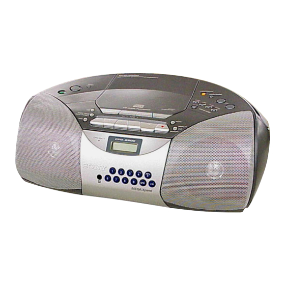
CFD-S400/S500
Photo: CFD-S500
SPECIFICATIONS
Model Name Using Similar Mechanism CFD-S36
CD
CD Mechanism Type
Section
Optical Pick-up Name
Model Name Using Similar Mechanism NEW
TC
Section Tape Transport Mechanism Type
Radio section
Frequency range
FM: 87.5 - 108 MHz
AM: 530 - 1,710 kHz
Antennas
FM: Telescopic antenna
AM: Built-in ferrite bar antenna
Cassette-corder section
Recording system
4-track 2 channel stereo
Fast winding time
Approx. 120 sec. with Sony cassette C-60
Frequency response
TYPE I (normal): 80 - 10,000 Hz
CD RADIO CASSETTE-CORDER
US Model
CFD-S500
Canadian Model
E Model
CFD-S400
KSM-213RDP
KSS-213R
MF-S200
– Continued on next page –
1
Advertisement
Table of Contents

Related Manuals for Sony CFD-S400


Summary of Contents for Sony CFD-S400
- Page 1 Recording system Other Specifications 4-track 2 channel stereo CD player section Fast winding time System Approx. 120 sec. with Sony cassette C-60 Compact disc digital audio system Frequency response Laser diode properties TYPE I (normal): 80 - 10,000 Hz Material: GaAlAs...
- Page 2 LES COMPOSANTS IDENTIFIÉS PAR UNE MARQUE 0 SUR LES DIAGRAMMES SCHÉMATIQUES ET LA LISTE DES PIÈCES SONT CRITIQUES POUR LA SÉCURITÉ DE FONCTIONNEMENT. NE REMPLACER CES COMPOSANTS QUE PAR DES PIÈCES SONY DONT LES NUMÉROS SONT DONNÉS DANS CE MANUEL OU DANS LES SUPPLÉMENTS PUBLIÉS PAR SONY.
-
Page 3: Table Of Contents
CFD-S400/S500 TABLE OF CONTENTS 1. SERVICING NOTES ............4 2. GENERAL ................5 3. DISASSEMBLY 3-1. Cabinet Top Assy ..............7 3-2. Cabinet Front Assy, Cabinet Rear Assy ......7 3-3. Wires ................... 8 3-4. MD Block ................8 3-5. Cassette Door Assy ............. 9 3-6. -
Page 4: Servicing Notes
CFD-S400/S500 SECTION 1 SERVICING NOTES LASER DIODE AND FOCUS SEARCH OPERATION CHUCK PLATE JIG ON REPAIRING CHECK 1. Turn ON the [POWER] button and press [CD] button to On repairing CD section, playing a disc without the lid (CD), use CD position. -
Page 5: General
CFD-S400/S500 SECTION 2 GENERAL This section is extracted from instruction manual. Location of controls Remote Control Inserting a cassette Loading a CD With the side you want SLEEP to play facing you POWER FUNCTION Number buttons With the labeled side up MODE ., >... -
Page 6: Disassembly
CFD-S400/S500 SECTION 3 DISASSEMBLY • The equipment can be removed using the following procedure. 3-1. CABINET TOP ASSY (Page 7) 3-2. CABINET FRONT ASSY, 3-10. CD LID 3-11. CD BLOCK ASSY CABINET REAR ASSY (Page 11) (Page 12) (Page 7) 3-12. -
Page 7: Cabinet Top Assy
CFD-S400/S500 Note : Follow the disassembly procedure in the numerical order given. 3-1. CABINET TOP ASSY 2 screw (2.6) handle 3 screw (2.6) CD lid 4 screw (2.6) 8 cabinet top assy 1 BTP 2.6x10 6 CNP804 5 CNP802 7 connector... -
Page 8: Wires
CFD-S400/S500 3-3. WIRES Put flat cable and wires between the cabinets and push them in the grooves located at A to E in the figure to prevent disconnection before assembling the set. from HEADPHONE board cabinet front cabinet rear 3-4. MD BLOCK 1 BVTP 2.6x10... -
Page 9: Cassette Door Assy
CFD-S400/S500 3-5. CASSETTE DOOR ASSY 1 BVTP 2.6x10 2 damper cassette spring flexible flat cable 3 cassette door assy 3-6. LCD BOARD, CONTROL (4) BOARD 1 BVTP (2.6) 6 LCD board 4 BVTP 2.6x10 5 claws 3 cassette holder 7 CONTROL (4) board... -
Page 10: Main Board
CFD-S400/S500 3-7. MAIN BOARD 6 BVTP 2.6x10 7 MAIN board 1 PWH 2.6x10 2 HEADPHONE board 3 CNP322 4 CNP902 5 CNP1 3-8. TUNER BOARD 2 telescopic antenna 1 B 3x8 4 BVTP 2.6x10 7 TUNER board 3 CNP1 5 claws... -
Page 11: Power Board
CFD-S400/S500 3-9. POWER BOARD 3 BVTP 2.6x10 4 BVTP 2.6x10 2 CNP901 6 POWER board 5 BVTP 2.6x10 1 CNP902 3-10. CD LID 3 CD lid CD spring 2 claw 1 claw... -
Page 12: Cd Block Assy
CFD-S400/S500 3-11. CD BLOCK ASSY 3 CD cover claws 4 CD block assy 1 PWH 2.6x10 2 PWH 2.6x10 3-12. OPTICAL PICK-UP 6 optical pick-up 5 sled shaft claw 1 gear (A) 2 PWB tapping (M2) 3 PWB tapping (M2) -
Page 13: R/P Head (Hrp301), Tc Board
CFD-S400/S500 3-13. R/P HEAD (HRP301), TC BOARD 4 Removal the solders. 2 BVTP 2x4 claws 3 TC board 1 R/P head (HRP301) 3-14. MOTOR ASSY (M801), MAIN BELT (B), SUB BELT (B) 6 motor assy (M801) 2 bind DT M2x6... -
Page 14: Mechanical Adjustments
CFD-S400/S500 SECTION 4 SECTION 5 MECHANICAL ADJUSTMENTS ELECTRICAL ADJUSTMENTS PRECAUTION TAPE SECTION 0 dB = 0.775 V 1. Clean the following parts with a denatured-alcohol-moistened swab : • Standard Output Level record/playback head pinch roller Output terminal HP OUT erase head rubber belts 32 Ω... -
Page 15: Tuner Section
CFD-S400/S500 TUNER SECTION 0 dB = 1 µV FM IF ADJUSTMENT • FM Section Adjust for a maximum reading on level meter. Setting: RADIO BAND•AUTO PRESET button: FM 10.7 MHz FM RF signal generator FM FREQUENCY COVERAGE TP (FM IN) ADJUSTMENT 0.01 µ... -
Page 16: Cd Section
CFD-S400/S500 Adjustment Location: CT3, L3 TRACKING ADJUSTMENT – MAIN board (component side) – TP (VT) (CONDUCTOR SIDE) CT1, L1 TP (FM IN) TRACKING (CONDUCTOR SIDE) ADJUSTMENT ADJUSTMENT FREQUENCY COVERAGE ADJUSTMENT ADJUSTMENT FREQUENCY COVERAGE ADJUSTMENT CD SECTION CD section adjustments are done automatically in this set. -
Page 17: Diagrams
CFD-S400/S500 SECTION 6 DIAGRAMS 6-1. IC PIN DESCRIPTION • IC802 uPD789477GC-A14-8BT (SYSTEM CONTROLLER) Pin No. Pin Name Pin Description Pin No. Pin Name Pin Description 1, 2 — Not used. (Open) Main system oscillation output (4.19 MHz) 3 to 5... -
Page 18: Block Diagram - Cd Section
CFD-S400/S500 6-3. BLOCK DIAGRAM — CD SECTION — CNP702 (2/2) LCHO INTERPOLATION CD_IN_ L SLICE ERROR MUTE DIGITAL FIN2 EFMIN (Page 19) LEVEL CORRECTION & FILTER CONTROL AUDIO CD ATTENUATION & RCHO CD_IN_R DEEMPHASIS 1-bit DAC PH/BH FIN1 RF AMP,... -
Page 19: Block Diagram - Main Section
CFD-S400/S500 6-4. BLOCK DIAGRAM — MAIN SECTION — R.RO VOLUME/SOUND PROCESSOR R.IN IC303 R.LINE CD_IN_R REC/PB POWER AMP IC304 PRE AMP (Page 18) R-CH IC301 L.RO J321 ALC 2 SEL2 TREBLE/ VIN2 VOUT2 L.LINE L.LO CD_IN_L BASS CONTROL HRP301 RECORD/PLAYBACK HEAD L.IN... -
Page 20: Printed Wiring Board - Cd Section
CFD-S400/S500 6-5. PRINTED WIRING BOARD — CD SECTION — • Refer to page 17 for Circuit Boards Location. THIS NOTE IS COMMON FOR PRINTED WIRING BOARDS AND SCHEMATIC DIAGRAMS. (In addition to this, the necessary note is printed in each block.) Common Note on Schematic Diagrams: •... -
Page 21: Schematic Diagram - Cd Section
CFD-S400/S500 6-6. SCHEMATIC DIAGRAM — CD SECTION — • Refer to page 20 for Common Note on Schematic Diagrams and page 35 for IC Block Diagrams. C727 C726 C724 C725 C721 R717 C730 C720 R716 C722 R718 R728 R727 C723... -
Page 22: Printed Wiring Board - Tuner Section
CFD-S400/S500 6-7. PRINTED WIRING BOARD — TUNER SECTION — • Refer to page 17 for Circuit Boards Location and page 20 for Common Note on Printed Wiring Boards. US,CND,E92,MX MODEL JC12 SP,KR MODEL (Page 24) US,CND,E92, (Page 24) MX MODEL... -
Page 23: Schematic Diagram - Tuner Section
CFD-S400/S500 6-8. SCHEMATIC DIAGRAM — TUNER SECTION — • Refer to page 20 for Common Note on Schematic Diagrams and page 36 for IC Block Diagrams. JC12 JC11 C51 C52 JC24 IC B/D IC B/D JC13 ANT1 CNP2 CNP1 (Page 25) -
Page 24: Printed Wiring Boards - Main Section
CFD-S400/S500 6-9. PRINTED WIRING BOARDS — MAIN SECTION — • Refer to page 17 for Circuit Boards Location and page 20 for Common Note on Printed Wiring Boards. • Semiconductor Location Ref. No. Location D322 D323 D324 D801 SP,KR MODEL... -
Page 25: Schematic Diagram - Main Section (1/2)
CFD-S400/S500 6-10. SCHEMATIC DIAGRAM — MAIN SECTION (1/2) — • Refer to page 20 for Common Note on Schematic Diagrams and page 37 for IC Block Diagrams. CNP806 CNP803 C106 C206 IC804 D801 R832 R835 R844 R839 (Page 28) R836... -
Page 26: Schematic Diagram - Main Section (2/2)
CFD-S400/S500 6-11. SCHEMATIC DIAGRAM — MAIN SECTION (2/2) — • Refer to page 20 for Common Note on Schematic Diagrams and page 37 for IC Block Diagrams. C327 C147 C247 IC B/D IC304 R150 C150 R140 IC303 R125 R149 R148... -
Page 27: Printed Wiring Board - Tc Section
CFD-S400/S500 6-12. PRINTED WIRING BOARD — TC SECTION — • Refer to page 17 for Circuit Boards Location and page 20 for Common Note on Printed Wiring Boards. • Semiconductor Location Ref. No. Location IC301 T301 C308 C307 Q301 C310... -
Page 28: Schematic Diagram - Tc Section
CFD-S400/S500 6-13. SCHEMATIC DIAGRAM — TC SECTION — • Refer to page 20 for Common Note on Schematic Diagrams and page 37 for IC Block Diagrams. IC301 R103 R112 IC B/D R301 C102 R102 C103 R104 R111 C301 C104 C101... -
Page 29: Printed Wiring Boards - Control Section
CFD-S400/S500 6-14. PRINTED WIRING BOARDS — CONTROL SECTION — • Refer to page 17 for Circuit Boards Location and page 20 for Common Note on Printed Wiring Boards. S408 • Semiconductor DISPLAY • S410 Location ENT• TAPE Ref. No. Location... -
Page 30: Schematic Diagram - Control Section
CFD-S400/S500 6-15. SCHEMATIC DIAGRAM — CONTROL SECTION — • Refer to page 20 for Common Note on Schematic Diagrams. (Page 25) CNP403 CNP404 CNP405 CNP401 CNP402 C401 S403 D401 S401 S409 S424 S428 R403 R415 R440 R401 R412 R423 Q401... -
Page 31: Printed Wiring Boards - Display Section
CFD-S400/S500 6-16. PRINTED WIRING BOARDS — DISPLAY SECTION — • Refer to page 17 for Circuit Boards Location and page 20 for Common Note on Printed Wiring Boards. • Semiconductor Location D405 Ref. No. Location OPR/BATT D405 LCD801 IC401 LIQUID CRYSTAL DISPLAY PANEL... -
Page 32: Schematic Diagram - Display Section
CFD-S400/S500 6-17. SCHEMATIC DIAGRAM — DISPLAY SECTION — • Refer to page 20 for Common Note on Schematic Diagrams. R448 R438 R445 R437 R444 R439 R443 D405 KH402 KH401 CNP406 S423 S422 S421 S420 S419 S418 S417 S416 R457 R456... -
Page 33: Printed Wiring Boards - Power Supply Section
CFD-S400/S500 6-18. PRINTED WIRING BOARDS — POWER SUPPLY SECTION — • Refer to page 17 for Circuit Boards Location and page 20 for Common Note on Printed Wiring Boards. • Semiconductor Location Ref. No. Location D901 D902 D903 (Page 24) -
Page 34: Schematic Diagram - Power Supply Section
CFD-S400/S500 6-19. SCHEMATIC DIAGRAM — POWER SUPPLY SECTION — • Refer to page 20 for Common Note on Schematic Diagrams. (Page 26) CNP902 CNP905 F902 T901 C906 JW902 C904 J901 C902 D904 D902 D903 D901 CNP901 C903 C901 CNB901... -
Page 35: Ic Block Diagrams
CFD-S400/S500 6-20. IC BLOCK DIAGRAMS IC701 LC78646E-E (CD Board) 78 77 76 75 74 73 72 71 69 68 67 66 65 64 63 62 61 FIN1 – FIN2 – TIN1 TBAL – – TIN2 – – TBAL – RFMON... - Page 36 CFD-S400/S500 IC702 BA5826FP-E2 (CD Board) IC1 TA2149BN (TUNER Board) GND1 FM RF-OUT FM RF SP– D.BUFF VCC1 FM RF-IN SL– AM RF-IN D.BUFF AM LOW CUT LEVEL D.BUFF SHIFT MIX OUT FM OSC D.BUFF SPIN LEVEL SHIFT AM OSC BUFF...
- Page 37 CFD-S400/S500 IC803 CAT24WC02JI-1.8-TE13 (MAIN Board) 1K BIT EEPROM ARRAY 8BIT 7BIT SLAVE • WORD ADDRESS DATA ADDRESS 7BIT DECODER REGISTER REGISTER START STOP CONTROL CIRCUIT HIGH VOLTAGE POWER SUPPLY OCCURENCE CIRCUIT VOLTAGE DETECTION IC303 BD3870FS-E2 (MAIN Board) TREBLE1 TREBLE2 BASS2...
-
Page 38: Exploded Views
CFD-S400/S500 SECTION 7 EXPLODED VIEWS NOTE: • The mechanical parts with no reference • Color Indication of Appearance Parts The components identified by mark 0 or dotted line with mark number in the exploded views are not supplied. Example : 0 are critical for safety. -
Page 39: Cabinet Front Section
CFD-S400/S500 7-2. CABINET FRONT SECTION SP301 MD block 60 59 LCD801 SP302 Ref. No. Part No. Description Remark Ref. No. Part No. Description Remark X-3381-559-1 DOOR SUB ASSY, CASSETTE * 63 A-3174-265-A DOOR ASSY, CASSETTE 3-237-694-31 HOLDER, CASSETTE 3-237-707-31 BUTTON, REC... -
Page 40: Cabinet Top Section
CFD-S400/S500 7-3. CABINET TOP SECTION S801 KSM-213RDP Ref. No. Part No. Description Remark Ref. No. Part No. Description Remark * 101 1-683-854-11 CONTROL (2) BOARD 3-923-736-01 COVER, CD 1-824-038-11 CABLE, FLEXIBLE FLAT 10P (CNP403) 3-931-379-21 RUBBER, VIBRATION PROOF 1-824-039-11 CABLE, FLEXIBLE FLAT 9P (CNP404) 3-921-725-11 SCREW (2.6X10), +PWH... -
Page 41: Cabinet Rear Section
CFD-S400/S500 7-4. CABINET REAR SECTION ANT1 T901 The components identified by Les composants identifiés par une mark 0 or dotted line with mark marque 0 sont critiques pour 0 are critical for safety. la sécurité. Replace only with part number Ne les remplacer que par une piéce... -
Page 42: Tape Mechanism Section
CFD-S400/S500 7-5. TAPE MECHANISM SECTION not supplied M801 HRP301 Ref. No. Part No. Description Remark Ref. No. Part No. Description Remark 3-244-086-01 ARM ASSY, PINCH ROLLER 3-237-719-01 CHASSIS, TC 3-244-079-01 BELT (B), SUB 3-030-741-01 SCREW (M2X2) 3-244-080-01 BELT (B), MAIN... -
Page 43: Cd Mechanism Section
CFD-S400/S500 7-6. CD MECHANISM SECTION (KSM-213RDP) not supplied not supplied not supplied The components identified by Les composants identifiés par une mark 0 or dotted line with mark marque 0 sont critiques pour 0 are critical for safety. la sécurité. -
Page 44: Electrical Parts List
CFD-S400/S500 SECTION 8 BATTERY (1) ELECTRICAL PARTS LIST BATTERY (2) NOTE: • Due to standardization, replacements in • Items marked “*” are not stocked since The components identified by mark 0 or dotted line with mark the parts list may be different from the they are seldom required for routine service. - Page 45 CFD-S400/S500 CONTROL (1) CONTROL (2) CONTROL (3) Ref. No. Part No. Description Remark Ref. No. Part No. Description Remark R703 1-216-835-11 METAL CHIP 1/10W S402 1-786-050-21 SWITCH, KEYBOARD (SLEEP) R704 1-216-835-11 METAL CHIP 1/10W ************************************************************* R705 1-216-835-11 METAL CHIP 1/10W...
- Page 46 CFD-S400/S500 CONTROL (3) CONTROL (4) HEADPHONE Ref. No. Part No. Description Remark Ref. No. Part No. Description Remark < TRANSISTOR > R433 1-216-829-11 METAL CHIP 4.7K 1/10W R434 1-216-813-11 METAL CHIP 1/10W Q401 8-729-029-13 TRANSISTOR DTC143ZUA-T106 R435 1-216-817-11 METAL CHIP...
- Page 47 CFD-S400/S500 MAIN Ref. No. Part No. Description Remark Ref. No. Part No. Description Remark < LIQUID CRYSTAL DISPLAY > C271 1-126-964-11 ELECT 10uF C321 1-104-665-11 ELECT 100uF LCD801 1-804-550-11 DISPLAY PANEL, LIQUID CRYSTAL C322 1-126-947-11 ELECT 47uF C323 1-126-964-11 ELECT 10uF <...
- Page 48 CFD-S400/S500 MAIN Ref. No. Part No. Description Remark Ref. No. Part No. Description Remark < DIODE > Q951 8-729-029-13 TRANSISTOR DTC143ZUA-T106 (SP,KR) Q952 8-729-040-76 TRANSISTOR KTA1273-Y-AT D322 8-719-988-61 DIODE 1SS355TE-17 Q953 8-729-029-13 TRANSISTOR DTC143ZUA-T106 D323 8-719-988-61 DIODE 1SS355TE-17 Q955 8-729-021-82 TRANSISTOR 2SD2396K...
- Page 49 CFD-S400/S500 MAIN Ref. No. Part No. Description Remark Ref. No. Part No. Description Remark R810 1-216-845-11 METAL CHIP 100K 1/10W R858 1-216-829-11 METAL CHIP 4.7K 1/10W R811 1-216-849-11 METAL CHIP 220K 1/10W R859 1-216-821-11 METAL CHIP 1/10W R812 1-216-845-11 METAL CHIP...
- Page 50 CFD-S400/S500 POWER Ref. No. Part No. Description Remark Ref. No. Part No. Description Remark 1-683-861-11 POWER BOARD C303 1-104-665-11 ELECT 100uF C304 1-126-947-11 ELECT 47uF ************* C305 1-162-962-11 CERAMIC CHIP 470PF 1-533-233-11 HOLDER, FUSE (CND,SP,KR) C306 1-162-970-11 CERAMIC CHIP 0.01uF...
- Page 51 CFD-S400/S500 TUNER Ref. No. Part No. Description Remark Ref. No. Part No. Description Remark R307 1-216-797-11 METAL CHIP 1/10W 1-164-230-11 CERAMIC CHIP 220PF R308 1-216-837-11 METAL CHIP 1/10W 1-162-927-11 CERAMIC CHIP 100PF R309 1-216-805-11 METAL CHIP 1/10W 1-162-919-11 CERAMIC CHIP...
- Page 52 CFD-S400/S500 TUNER Ref. No. Part No. Description Remark Ref. No. Part No. Description Remark 1-216-864-11 METAL CHIP 1/10W MISCELLANEOUS JC11 1-216-864-11 METAL CHIP 1/10W *************** JC12 1-216-864-11 METAL CHIP 1/10W JC13 1-216-864-11 METAL CHIP 1/10W 1-452-899-11 MAGNET JC24 1-216-864-11 METAL CHIP...
- Page 53 CFD-S400/S500 MEMO...
- Page 54 CFD-S400/S500 REVISION HIST ORY Clicking the version allows you to jump to the revised page. Also, clicking the version at the upper on the revised page allows you to jump to the next revised page. Ver. Date Description of Revision...