Pioneer CDJ-800MK2 Service Manual
Compact disc player
Hide thumbs
Also See for CDJ-800MK2:
- Operating instructions manual (116 pages) ,
- Service manual (114 pages) ,
- Operating instructions manual (60 pages)
Table of Contents
Advertisement
COMPACT DISC PLAYER
CDJ-800MK2
THIS MANUAL IS APPLICABLE TO THE FOLLOWING MODEL(S) AND TYPE(S).
Model
Type
CDJ-800MK2
KUCXJ
CDJ-800MK2
WYXJ5
CDJ-800MK2
RLFXJ
For details, refer to "Important symbols for good services" .
PIONEER CORPORATION
PIONEER ELECTRONICS (USA) INC. P.O. Box 1760, Long Beach, CA 90801-1760, U.S.A.
PIONEER EUROPE NV Haven 1087, Keetberglaan 1, 9120 Melsele, Belgium
PIONEER ELECTRONICS ASIACENTRE PTE. LTD. 253 Alexandra Road, #04-01, Singapore 159936
PIONEER CORPORATION 2006
Power Requirement
AC 120 V
AC 220 – 240 V
AC 110-120 V / 220-240 V
4-1, Meguro 1-chome, Meguro-ku, Tokyo 153-8654, Japan
CDJ-800MK2
T-ZZR JUNE 2006 printed in Japan
ORDER NO.
RRV3364
Remarks
Advertisement
Chapters
Table of Contents

Related Manuals for Pioneer CDJ-800MK2


Summary of Contents for Pioneer CDJ-800MK2
- Page 1 PIONEER CORPORATION 4-1, Meguro 1-chome, Meguro-ku, Tokyo 153-8654, Japan PIONEER ELECTRONICS (USA) INC. P.O. Box 1760, Long Beach, CA 90801-1760, U.S.A. PIONEER EUROPE NV Haven 1087, Keetberglaan 1, 9120 Melsele, Belgium PIONEER ELECTRONICS ASIACENTRE PTE. LTD. 253 Alexandra Road, #04-01, Singapore 159936...
-
Page 2: Safety Information
The use of a substitute replacement component which does Leakage 0.5mA current Device not have the same safety characteristics as the PIONEER tester under recommended replacement one, shown in the parts list in test this Service Manual, may create shock, fire, or other hazards. - Page 3 CLASS 1. A specially instructed person should servicing operation of the apparatus. LABEL CHECK CDJ-800MK2 WYXJ5 and KUCXJ : Types Only for RLFXJ (DRW2308) (DRW2248) Additional Laser Caution 1.
- Page 4 To protect products from damages or failures during transit, the shipping mode should be set or the shipping screws should be installed before shipment. Please be sure to follow this method especially if it is specified in this manual. CDJ-800MK2...
-
Page 5: Table Of Contents
6. ADJUSTMENT ..............................85 7. GENERAL INFORMATION ..........................86 7.1 DIAGNOSIS..............................86 7.1.1 SERVICE MODE ..........................86 7.1.2 RESET and CLOCK MAP ........................92 7.1.3 TROBLE SHOOTING .........................94 7.1.4 POWER ON SEQUENCE ........................105 7.1.5 DISASSEMBLY ..........................106 7.2 PARTS ..............................114 7.2.1 IC..............................114 8. PANEL FACILITIES ............................140 CDJ-800MK2... -
Page 6: Specifications
• Power cord ..............1 • Audio cable ..............1 • Control cable ..............1 • Forced eject pin (housed in a groove in the bottom panel)... 1 NOTE: Specifications and design are subject to possible modification with-out notice. CDJ-800MK2... - Page 7 Accessories Power Cord Audio Cable Forced Fject Pin (ADG7021 : KUCXJ) (VDE1064) L=1.5m (housed in a groove in (ADG7097 : RLFXJ) the bottom panel) (DEX1008) (ADG1154 : WYXJ,RLFXJ) Control Cord (XDE3063) L=1 m CDJ-800MK2...
-
Page 8: Exploded Views And Parts List
For the applying amount of lubricants or glue, follow the instructions in this manual. (In the case of no amount instructions, apply as you think it appropriate.) 2.1 PACKING KUCXJ & RLFXJ types only WYXJ & RLFXJ type only KUCXJ type only CDJ-800MK2... - Page 9 Label See Contrast table(2) Pad B DHA1556 Pad C DHA1557 Pad D DHA1558 (2) CONTRAST TABLE CDJ-800MK2/KUCXJ, /WYXJ5 and RLFXJ types are constructed the same except for the following: CDJ-800MK2/ CDJ-800MK2/ CDJ-800MK2/ Mark No. Symbol and Description KUCXJ WYXJ5 RLFXJ >...
-
Page 10: Exterior Section
2.2 EXTERIOR SECTION Refer to "2.3 CONTROL PANEL SECTION". 31x4 33x4 9-(b) Refer to "2.4 SLOT-IN MECHANISM SECTION". 46x4 CDJ-800MK2... - Page 11 Silicon Lubber D5 L DEB1456 Screw IPZ30P100FTC Bottom Cushion S4 DEC2506 Heat Sink DNG1102 (2) CONTRAST TABLE CDJ-800MK2/KUCXJ, /WYXJ5 and RLFXJ types are constructed the same except for the following: CDJ-800MK2/ CDJ-800MK2/ CDJ-800MK2/ Mark No. Symbol and Description KUCXJ WYXJ5 RLFXJ >...
-
Page 12: Control Panel Section
2.3 CONTROL PANEL SECTION Grease: GYA1001( ZLB-PN397B) 56x3 28x9 17x3 10x3 13x12 38-(a) 38-(b) 38-(c) 48-2 30x8 54x2 48-1 CDJ-800MK2... - Page 13 Set Knob (Eject) DAC2287 CALL Knob DAC2289 RELOOP Knob DAC2291 Slide Knob DAC2292 TEXT/A.CUE Knob DAC2294 Folder Search Knob DAC2298 DEL/MEMO Knob DAC2299 Reverse Knob DAC2364 Slide Sheet (gray) DAH2374 Display Panel DAH2418 Earth Plate (CU) DBK1224 Vessel Sheet DEC2495 CDJ-800MK2...
-
Page 14: Slot-In Mechanism Section
Cleaning paper : GED-008 RLYB CN12 (Pickup) RLYB CN16 (Loading Motor) Grease GYA1001 RLYB CN14 (Stepping Motor) (ZLB-PN397B) Note: The TM. Assy 03-S is supplied only in assembly form, not as a single part. To MAIN CN102 (Spindle Motor) CDJ-800MK2... - Page 15 DNK4371 Gear Holder SV DNK4372 Clamper 04 Assy DXB1859 Screw BPZ20P060FTC Floating Rubber (SI) VEB1351 Float Base 04 Assy DXB1838 Spacer POR (T3) DEB1566 Vessel Cushion A DEC2852 Vessel Cushion B DEC2853 Vessel Cushion C DEC2854 Front Sheet DED1132 CDJ-800MK2...
-
Page 16: Block Diagram And Schematic Diagram
MECHANISM SV MAIN ASSY ASSY NJM2885DL1 CN301 BA008C0WCP CN301 BA008C0WCP CN53 CN52 REGB ASSY V+10B V+7A CN53 V+6B V+3D For KUCXJ, WYXJ5 SECB ASSY CN51 CN22 CN56 ACIN ASSY TRNS ASSY For RLFXJ BROWN CN50 VIOLET BLUE ACIN ASSY CDJ-800MK2... - Page 17 DSPC56371AF180-K IC301 SCF5249VM140-K JA801 DKB1053 IC801 OP AMP AUDIO OUT CN701 CN801 JA802 PKB1033 IC702 PE8001A IC304 DIGITAL OUT BU4230G CN802 CN602 CN1601 CN601 JOGB ASSY DFLB ASSY CN500 CN501 JFLB ASSY CN600 CN1503 CN503 CN502 CN1502 KSWB ASSY CDJ-800MK2...
-
Page 18: Block Diagram (2)
FLAC_J 3PIN DATA Cntrol CDJ-800MK2 has two MPU, MPU (MAIN), DISPLAY-MPU (DFLB). One controls CORE BLOCK, Another is Top panel about DISPLAY, LED, VOLUME, S ACIN ASSY RESET IC and X'TAL have on the MAIN ASSY too. It has two MEMORY. One 64MB sized SDRAM, Another is 8MB sized FLASH MEMOR About POWER BLOCK, Please refer to POWER DELIVERY MAP. - Page 19 DWG1623 VYNIL IC501 DISPLAY (MASK) RESET IC 16.00MHz SLIDER V501 DATA FL JOGB ASSY DWG1625 R to R 13PIN DATA Cntrol (DFLB). ISPLAY, LED, VOLUME, SW, JOG, etc. JFLB ASSY DWG1624 Rotation Detect 8MB sized FLASH MEMORY. Y MAP. CDJ-800MK2...
-
Page 20: Block Diagram (Power)
<5.0A <1.5A IC54 IC25 IC25 Vload +32V <200mA <200mA <630mA <630mA IC58 IC59 FLAC_D FLAC_J DATA Cntrol Regurator supporting Current Shutdown 3.3V 3.3V 15W POINT IC Protect Before REG-IC Pori SW ACIN ASSY FUSE Screw (Chasis GND) MAX SPEC CDJ-800MK2... - Page 21 GNDD VYNIL GNDF GNDF EarthPlate ChasisGND GNDF GNDF GNDAD GNDAD DISPLAY C506 C506 GNDD GNDD SLIDER JOGB ASSY GNDD GNDD DWG1625 V+5P DATA Cntrol 15W POINT Before REG-IC <200mA IC603 JFLB ASSY DWG1624 Rotation Detect Screw (Chasis GND) Q604 CDJ-800MK2...
-
Page 22: Overall Wiring Diagram
3.4 OVERALL WIRING DIAGRAM (Loading Motor Assy-S) DXX2510 SLOT-IN RLYB ASSY SLMB ASSY TRNS ASSY ACIN ASSY DWR1429(WYXJ5) DWR1430(KUCXJ) (RLFXJ) (KUCXJ, WYXJ5) SECB ASSY ACIN ASSY REGB ASSY DWR1432(RLFXJ) CDJ-800MK2... - Page 23 MAIN ASSY ( 1/3 – 3/3) JACK ASSY JFLB ASSY DFLB ASSY KSWB ASSY CDJ-800MK2...
-
Page 24: Main (1/3) And Rlyb Assys
3.5 MAIN (1/3) and RLYB ASSYS MAIN ASSY (DWG1622) (TS) (TS) (TS) (RF) (RF) (RF) (RF) (RF) (RF) (TS) (TS) (TS) CDJ-800MK2... - Page 25 (TS) : TRACKING SERVO LOOP LINE : STEPPING SERVO LOOP LINE (RF) (RF) (RF) (RF) (TD) (TD) (TS) (TS) CN1901 to LOADING MOTOR to STEPPER MOTOR RLYB ASSY (DWX2602) : The Power supply is shown with the marked box. CDJ-800MK2...
-
Page 26: Main Assy(2/3)
3.6 MAIN ASSY(2/3) MAIN ASSY (DWG1622) (1/2) Large size CN53 SCH diagram (Data) (Data) : PANEL DATA (Digital) CDJ-800MK2... - Page 27 CDJ-800MK2...
- Page 28 MAIN ASSY (DWG1622) (2/2) Large size SCH diagram (Data) (Data) (Data) (Data) to ICE BOARD CDJ-800MK2...
- Page 29 (Data) : PANEL DATA (Digital) CDJ-800MK2...
-
Page 30: Main Assy(3/3)
3.7 MAIN ASSY(3/3) MAIN ASSY (DWG1622) CDJ-800MK2... - Page 31 (Ana) (Ana) : The Power supply is shown with the marked box. (Data) : AUDIO DATA (Digital) (Ana) : AUDIO Lch OUT (Analog) : DATA AUDIO OUT (Digital) CDJ-800MK2...
-
Page 32: Ac In, Trns, Secb And Regb Assys
3.8 AC IN, TRNS, SECB and REGB ASSYS DWR1439 (KUCXJ) ACIN ASSY DWR1429 (WYXJ5) DWR1371 (KUCXJ, WYXJ5) TRNS ASSY DWR1428 (RLFXJ) ACIN ASSY DWR1432 (RLFXJ) KUCXJ WYXJ5 RLFXJ DWR1371 DWR1371 CDJ-800MK2... - Page 33 SECB ASSY (DWR1309) REGB ASSY (Data) (Data) (Data) (Data) (Data) : AUDIO DATA (Digital) : The Power supply is shown with the marked box. CDJ-800MK2...
-
Page 34: Dflb, Jack And Kswb Assys
3.9 DFLB, JACK and KSWB ASSYS DFLB ASSY (DWG1623) (Data) (Data) (Data) CDJ-800MK2... - Page 35 KSWB ASSY (DWS1386) JACK ASSY (DWG1626) (Ana) (Ana) : The Power supply is shown with the marked box. (Data) : PANEL DATA (Digital) (Ana) : AUDIO Lch OUT (Analog) : DIGITAL AUDIO OUT (Digital) CDJ-800MK2...
-
Page 36: Jflb, Sldb, Slmb And Jogb Assys
3.10 JFLB, SLDB, SLMB and JOGB ASSYS JFLB ASSY (DWG1624) CDJ-800MK2... - Page 37 : The Power supply is shown with the marked box. : The Power supply is shown with the marked box. SLDB ASSY (DWS1387) SLDB ASSY (DWS1387) SLMB ASSY (DWS1388) SLMB ASSY (DWS1388) JOGB ASSY (DWG1625) JOGB ASSY (DWG1625) CDJ-800MK2...
-
Page 38: Waveforms
CH3 : TE V: 2.0 V/div. H: 100 msec/div. V: 5.0 V/div. H: 500 msec/div. V: 1.0 V/div. H: 200 msec/div. CH4 : LO– CH4 : DMO V: 5.0 V/div. H: 500 msec/div. V: 2.0 V/div. H: 200 msec/div. CDJ-800MK2... - Page 39 Conditions: At the time of power on, a - b : 370 msec a - c : 636 msec without a disc loaded a -d : 1 182 msec Reset clear e - a : 70 msec 3.3 V 3.3 V 3.3 V 3.3 V CDJ-800MK2...
- Page 40 Conditions: At the time of power on, without a disc loaded a - b : 69 msec a - c : 442 msec a - b : 1 256 msec a - b : 680 msec a - c : 1 318 msec b - c : 373 msec CDJ-800MK2...
- Page 41 • The MPU polls the audio DSP and DAC in a fixed cycle. • The intervals of a cycle are 3 msec for playback of a CD-DA, and 10 msec for playback of a signal for MP3. Between musical pieces Power ON PLAY start CDJ-800MK2...
- Page 42 V: 2.0 V/div. H: 1 sec/div. CH2 : JDATA Data Line CH2 : JDATA Data Line V: 2.0 V/div. H: 100 µsec/div. V: 2.0 V/div. H: 1 sec/div. Conditions: 10 POINTS × 1 disc Conditions: 10 POINTS × 1 disc Expansion Expansion CDJ-800MK2...
- Page 43 - b : 169.5 msec Conditions: At the time of power on, a - c : 679.7 msec Conditions: During playback without a disc loaded a - d : 1 186.4 msec Expansion A Expansion B Expansion C Expansion D Power ON CDJ-800MK2...
- Page 44 V: 5.0 V/div. H: 2 msec/div. CH3 : JSDO V: 5.0 V/div. H: 2 msec/div. CH4 : JSCLK V: 5.0 V/div. H: 2 msec/div. Conditions: With a disc loaded, during playback Expansion A Expansion B Expansion C Expansion D CDJ-800MK2...
-
Page 45: Voltages
Note that the result of measurement of a waveform comprising many AC-current components will vary from tester to tester. Conditions of measurement: Play back Track 2 of the STD-905 Test Disc from Pioneer. • For the IC mounted on the SECB Assy, measurement is performed with loads at the downstream stages lifted. - Page 46 Voltage (V) Pin No. Voltage (V) Pin No. Voltage (V) Pin No. Voltage (V) Pin No. Voltage (V) 0–1.8 1.9–2.2 1–4.5 1–4.5 1.6–1.8 0.5–0.7 0.5–0.7 0.5–0.7 0.7–0.9 0.7–0.9 0.5–0.7 0.4–0.7 0.6–0.9 0.4–0.8 0.5–0.7 0.5–0.7 0.5–0.7 0.8–1.0 0.6–0.8 0.5–0.8 0.5–0.8 CDJ-800MK2...
- Page 47 1.2–1.5 0.8–1.1 0.5–0.7 0.5–0.8 IC309 TC7SET08FUS1 0.5–0.8 Pin No. Voltage (V) IC703 BD00KA5WFP Pin No. Voltage (V) 0.4–0.7 0.8–1.0 0.5–0.7 IC310 TC7WU04FU 0.5–0.8 Pin No. Voltage (V) IC704 NJM2880U1-05 Pin No. Voltage (V) IC304 BU4230G Pin No. Voltage (V) CDJ-800MK2...
- Page 48 Voltage (V) Pin No. Voltage (V) -2.7 -6.1 -7.0 -5.7 IC052 TC7S04FU Pin No. Voltage (V) IC057 BA50BC0WFP Pin No. Voltage (V) 1.4–1.8 REGB ASSY IC091 BA00BC0WCP-V5 Pin No. Voltage (V) IC092 BA00BC0WCP-V5 Pin No. Voltage (V) 11.2 11.2 CDJ-800MK2...
-
Page 49: Pcb Connection Diagram
Symbol In PCB Symbol In Schematic Part Name Diagrams Diagrams C E B Capacitor Connector Transistor B C E SIDE A Transistor with resistor B C E Field effect SIDE B Chip Part P.C.Board transistor Resistor array 3-terminal regulator CDJ-800MK2... -
Page 50: Main Assy
SPINDLE MOTOR CN53 CN102 CN301 IC304 IC308 Q301 Q305 Q302 IC302 Q706 IC300 IC305 IC308 Q303 Q305 Q304 IC302 Q705 IC104 IC304 Q301 IC309 Q302 Q706 IC300 IC305 Q303 IC309 Q304 Q705 IC104 IC307 IC301 IC306 IC307 IC301 IC306 CDJ-800MK2... - Page 51 SIDE A CN1101 NOTE : The encircled numbers denote measuring point. CN101 (DNP2131-C) Q101 IC105 IC703 IC106 IC702 IC704 IC100 IC104 Q101 IC105 IC703 IC106 IC702 IC704 IC102 IC701 IC100 IC104 IC701 IC102 CDJ-800MK2...
- Page 52 SIDE B MAIN ASSY CN101 Q707 IC101 IC103 Q707 IC101 IC103 CDJ-800MK2...
- Page 53 SIDE B CN301 CN102 (DNP2131-C) IC303 IC311 IC310 IC312 IC311 IC310 NOTE : The encircled numbers denote measuring point. IC303 IC312 CDJ-800MK2...
-
Page 54: Rlyb Assy
4.2 RLYB ASSY SIDE A SIDE A RLYB ASSY CN101 PICKUP ASSY (CN1) LOADING MOTOR CN1901 STEPPER MOTOR (DNP2131-C) CDJ-800MK2... - Page 55 SIDE B SIDE B RLYB ASSY C 1 1 0 5 C 1 1 0 7 (DNP2131-C) CDJ-800MK2...
-
Page 56: Secb Assy
W472 2.FLAC2 3.GND 3.V-7 1.FLAC1 CAUTION 4.GND 2.V+8 5.GND 6.FLAC3 1.V+8 REPLACE IC 7.GND 8.FLAC4 MFD.BY LITTE JA52 9.XRST 10.V+5 11.TSDI 12.V7AL 13.TSCS 14.GND 15.TSDO 16.VLDD 17.TSCLK V+5P W458 V+7M W449 W448 W447 V+5P CN50 CN56 CN56 CN802 CN501 CDJ-800MK2... - Page 57 SIDE A IC53 IC54 IC61 IC58 IC50 ATTENTION CAUTION SECB REMPLACER LE IC LINK REPLACE IC LINKS AS MARKED. COMME INDIQUE. DWR1309 MFD.BY LITTELFUSE INC. DE CHEZ LITTELFUSE INC. W701 CONTACT SIDE CN53 IC59 IC60 W452 V+6B (DNP2132-C) CN53 CN301 CDJ-800MK2...
- Page 58 0 1 2 3 4 5 6 7 8 9 3.GN 4.GND 5.GND -GNDS- 6.FLAC3 7.GND -GNDD- 8.FLAC4 9.XRST 10.V+5 -GNDM- 11.TSDI 12.V7AL IC55 13.TSCS -V+3D- 14.GND 15.TSDO SECB -V+7M- 16.VLDD 17.TSCLK DWR1309 -V+6B- CN53 IC57 -V+8- -V+5P- CN53 (DNP2132-C) CDJ-800MK2...
- Page 59 1.FLAC1 IC56 1.FLAC2 2.FLAC1 IC51 IC51 3.GND ADD SOLDER 4.GND 3.V-7 5.GND 6.FLAC3 2.V+8 7.GND 1.V+8 8.FLAC4 9.XRST 10.V+5 11.TSDI 12.V7AL 13.TSCS 14.GND 15.TSDO IC52 16.VLDD IC52 17.TSCLK IC57 CN50 CN56 NOTE : The encircled numbers denote measuring point. CDJ-800MK2...
-
Page 60: Trns Assy
SIDE A SIDE A TRNS ASSY CN 1 (KUC/JJ, DWR1371 WY/WA) W514 W513 DWR1428 (RLF) TRNS ICP21 491005 491.630 ICP25 491005 ICP22 11.V+6B 10.GND 9.V+10B 8.GND CN51 7.GND 6.GND 5.VLD 4.FLAC4 3.FLAC3 2.FLAC2 1.FLAC1 (DNP2132-C) IC22 IC21 IC25 IC23 IC24 CDJ-800MK2... - Page 61 SIDE B SIDE B TRNS ASSY ADD SOLDER IC25 11.V+6B 10.GND 9.V+10B 8.GND 7.GND 6.GND 5.VLD 4.FLAC4 3.FLAC3 2.FLAC2 1.FLAC1 CN22 (DNP2132-C) IC24 IC23 IC25 IC21 IC22 CDJ-800MK2...
-
Page 62: Ac In Assys
4.5 AC IN ASSYS SIDE A SIDE A ACIN ASSY T AL NEUTRAL W500 W501 FU8001 RISK OF FIRE - REPLACE FUSE W498 DWR1429 MARKED. W497 DWR1430 W496 DWR1431 LIVE W495 DWR1432 POWER SW ACIN PRIMARY FU8001 W8001 LITTELFUSE INC. 21801.6 (DNP2132-C) CDJ-800MK2... - Page 63 SIDE B SIDE B ACIN ASSY NEUTRAL LIVE POWER SW 2.NEUTRAL ADD SOLDER 1.LIVE 220-240V ACIN 3.NEUTRAL 2.220-240V 1.110-120V 100-110V PRIMARY (DNP2132-C) CDJ-800MK2...
-
Page 64: Dflb Assy
FL HOLDER D506 W587 W551 TEXT TIME S503 D507 S510 S509 W536 W535 D503 D504 D502 D501 S504 D508 S513 RELOOP D512 LOOP-IN LOOP-OUT S512 S511 W523 CN500 W525 W524 S514 D510 D511 CN600 W511 W510 CN502 CN502 CN1502 CDJ-800MK2... - Page 65 W607 DELL W606 S507 W578 S508 W577 W576 W575 W579 <CALL CALL> W574 W544 S505 S506 X501 S515 S516 W548 W549 C506 S517 D509 CN503 QUICK RETURN 1.GNDF 2.V5AD 3.ADIN 4.ADCT 5.GNDAD 6.JVOL 7.KEY1SL 8.VINL 9.MTL 10.TEMPOL 11.GND (DNP2132-C) CDJ-800MK2...
- Page 66 DELL C522 C525 R512 C527 R521 XRST CALL> IC502 CNVSS R522 X501 1.GNDF <CALL 2.V5AD 3.ADIN R500 QUICK C532 C533 RETURN 4.ADCT V5AD S516 D509 5.GNDAD R559 S515 Q508 6.JVOL S513 RELOO /EXIT Q510 7.KEY1SL 8.VINL 9.MTL 10.TEMPOL 11.GND CDJ-800MK2...
- Page 67 Q507 8.JSCLK 7.TCH 6.VLDD S513 LOOP-IN LOOP-OUT D512 RELOOP /EXIT 5.JOG1 4.GND 3.JOG2 2.GND CN500 1.V+5 8.CLED 7.PLED 6.V7AL CONTACT 5.GND SIDE 4.GNDAD 3.CUE Q509 2.PLAY 1.KEY0 V7AL CN502 CN500 CN502 NOTE : The encircled numbers denote measuring point. CDJ-800MK2...
-
Page 68: Regb And Jack Assys
REGB ASSY IC92 IC91 IC92 IC91 W503 W504 DWR1310 REGB (DNP2132-C) CN52 JACK ASSY JA802 JA801 C804 C834 W488 C803 C833 IC801 IC801 W466 W461 C801 C831 W460 W465 W463 W467 W462 W464 CN701 W454 W453 CN802 (DNP2132-C) CN802 CN50 CDJ-800MK2... - Page 69 SIDE B SIDE B REGB ASSY (DNP2132-C) JACK ASSY DOUT Q832 C812 Q802 Q802 Q801 R816 Q831 Q831 CN802 (DNP2132-C) CN801 CN802 NOTE : The encircled numbers denote measuring point. CDJ-800MK2...
-
Page 70: Kswb Assy
4.8 KSWB ASSY SIDE A SIDE A KSWB ASSY KSWB DWS1386 S1501 PLAY D1504 D1503 S1502 D1502 D1501 W516 W505 W506 S1506 S1505 SEARCH-F SEARCH-R W502 W499 S1504 S1503 T-SEARCH-F W489 T-SEARCH-R W478 CN1502 CN502 (DNP2132-C) CDJ-800MK2... - Page 71 SIDE B SIDE B KSWB ASSY PLAY Q1502 Q1502 KSWB DWS1386 Q1501 Q1501 SEARCH-F SEARCH-R T-SEARCH-F T-SEARCH-R (DNP2132-C) CN1502 CN1502 CDJ-800MK2...
-
Page 72: Jflb Assy
REPLACE IC 3.JBK MFD.BY LITTELFU 4.JXSTB 5.JSDO 6.JSCLK ATTENT 7.TCH 8.VLDD 9.JOG1 REMPLACER LE I 10.GNDD COMME INDIQUE 11.JOG2 12.GNDD DE CHEZ LITTELF 13.V+5V V601 W135 W122 VLDJ VLDJ C601 W123 W121 W120 VLDJ CN601 CN601 CN1601 Production code CDJ-800MK2... - Page 73 SIDE A AUTION IC603 PLACE IC LINKS AS MARKED. D.BY LITTELFUSE INC. ATTENTION DWG1624 Q604 MPLACER LE IC LINK MME INDIQUE. JFLB CHEZ LITTELFUSE INC. IC601 GNDD Q603 Q602 W126 1.TCH W119 2.NC Q601 3.GNDD SHEET SW code (DNP2133-D) CDJ-800MK2...
- Page 74 SIDE B JFLB ASSY DWG1624 GNDD 3.GNDD 2.NC 1.TCH CN602 0 1 2 3 (DNP2133-D) CDJ-800MK2...
- Page 75 4.JXSTB 5.JSDO 6.JSCLK 7.TCH 8.VLDD 9.JOG1 10.GNDD 11.JOG2 12.GNDD 13.V+5V IC602 VLDJ VLDJ VLDJ CN601 CN601 NOTE : The encircled numbers denote measuring point. 0 1 2 3 4 5 6 7 8 9 0 1 2 3 NP2133-D) CDJ-800MK2...
-
Page 76: Sldb Assy
4.10 SLDB ASSY SIDE A SLDB ASSY S1551 SLDB DWS1387 D1553 VR1551 W103 W101 SIDE B CN1503 SLDB ASSY CN1503 GNDF GNDF ADIN C1560 ADCT R1565 V5AD GNDF GNDAD R1563 VR1552 V5AD GNDAD D1551 VINYL SPEED ADJUST S1552 S1551 ADD SOLDER CDJ-800MK2... - Page 77 D1552 V5AD W111 W116 GNDAD GNDF D1551 W102 VR1552 VINYL SPEED ADJUST (DNP2133-D) SIDE B SLDB DWS1387 ADD SOLDER VR1551 ADCT V5AD C1555 D1560 GNDAD GNDF GNDAD ADIN S1551 D1561 (DNP2133-D) NOTE : The encircled numbers denote measuring point. CDJ-800MK2...
-
Page 78: Slmb And Jogb Assys
4.11 SLMB and JOGB ASSYS SIDE A SIDE A SLMB ASSY SLOTSW SLOTSW JOGB ASSY JOGB DWG1625 CN1601 3.LPS2 2.GND 1.LPS1 (DNP2133-D) (DNP2133-D) CN1601 CN601 CDJ-800MK2... - Page 79 SIDE B SIDE B SLMB ASSY SLOTSW SLOTSW JOGB ASSY R1601 3.LPS2 2.GND 1.LPS1 (DNP2133-D) (DNP2133-D) CN1601 CDJ-800MK2...
-
Page 80: Pcb Parts List
Ex.2 When there are 3 effective digits (such as in high precision metal film resistors). 5.62k Ω 562 x 10 5621 RN1/4PC 5 6 2 1 7 7 7 7 LIST OF HOLE PCB ASSEMBLIES CDJ-800MK2/ CDJ-200MK2/ CDJ-800MK2/ Mark Symbol and Description KUCXJ WYXJ5 RLFXJ 1..MOTHER ASSY... - Page 81 7 7 7 7 PCB PARTS LIST FOR CDJ-800MK2 UNLESS OTHER WISE NOTED Mark No. Description Part No. Mark No. Description Part No. C161–C164, C307, C309, C312 CKSRYB104K16 C314, C318, C319, C322–C335 CKSRYB104K16 MAIN ASSY C339–C348, C350–C355 CKSRYB104K16 C358, C359, C361, C363, C366...
- Page 82 IC25 (630 mA) AEK7006 > IC23, IC24 (3.5 A) AEK7017 > IC21, IC22 (5.0 A) AEK7019 OTHERS > D25–D28 1SR154-400 H1, H2 FUSE CLIP AKR1004 > D21–D24 RB060L-40 > CN1 2P-VH CONNECTOR B2P3-VH > AN1 AS INLET 1P XKP3042 CDJ-800MK2...
-
Page 83: Regb Assy
X501 (16.0 MHz) DSS1149 C802, C809, C832 CKSRYB104K16 C801, C804, C831, C834 CQMBA102J50 C806, C808, C836, C838 CQMBA152J50 SWITCHES AND RELAYS S501–S504, S511–S514 DSG1079 S505–S510, S515–S517 VSG1024 RESISTORS R806, R836 RN1/16SE1102D Other Resistors RS1/16S###J CAPACITORS C532, C533, C538 CCSRCH120J50 CDJ-800MK2... - Page 84 Q602, Q603 2SC1815 Q604 2SD1858X D603 1SS355 D604 UDZS13(B) D605 UDZS15(B) D601 UDZS8R2(B) CAPACITORS C611–C614 CCSRCH221J50 C601 CEHAR100M16 C600, C602 CEHAR101M10 C606 CEHAR220M35 C608 CEHAR330M10 C607 CKSRYB102K50 C603, C605, C609 CKSRYB103K50 C604 CKSRYF104Z50 RESISTORS R600 RD1/2VM680J Other Resistors RS1/16S###J CDJ-800MK2...
-
Page 85: Adjustment
Goes out the ring B of JOG-FL when the volume position is less than the center. And SLIDER VOLUME light it when it is more than the center. To decrease To increase the load the load JOG Check Mode : CANCEL POWER OFF CDJ-800MK2... -
Page 86: General Information
All FL lights up All LED lights up MEMORY MEMORY EJECT EJECT CUE/LOOP CALL < CALL < CUE/LOOP CALL > CALL > REVERSE REVERSE TOUCH SENSOR TOUCH SW JOG rotating to FWD JOG > JOG rotating to REV < JOG CDJ-800MK2... - Page 87 It is necessary to make it rotate top speed to 7.0 or more times to measure the rotation fall time required. When it carries out continuously several times, the time which took the average with a part for greatest ever 4 time is displayed 2nd henceforth. Measurement which absorbed variation can be performed by performing this. CDJ-800MK2...
- Page 88 The product does not judge whether they are inferior goods at the time of service. Eject A disk is ejected. Mode Change If the MASTER TEMPO button is pushed into player operation mode, MASTER TEMPO LED will light up, and it will shift to the below-mentioned "test operation mode." CDJ-800MK2...
- Page 89 If the MASTER TEMPO button is pushed into "player operation mode", MASTER TEMPO LED will light up, and it will shift to the below-mentioned "test operation mode." ∗ When you rise at a step in test mode, please input a command in order of "Servo All Off", "Focus On", and "Spindle Kick, Tracking On." CDJ-800MK2...
-
Page 90: How To Upgrade The Software Of The Microcomputer
However, the program is stored in FLASH-ROM of a player microcomputer, and has structure transmitted to each processor from a player microcomputer at the time of a power supply ON. • How to upgrade the software of the microcomputer AUTO CDJ-800Mk2 POWER QUICK RETURN FL Display... - Page 91 ∗ CAUTIONT There is a function which carries out the memory of the CUE/LOOP point for the 800 maximum disks in this machine. If an error history is cleared, since all CUE/LOOP memories will also be cleared simultaneously, please take great care about use in this mode. CDJ-800MK2...
-
Page 92: Reset And Clock Map
7.1.2 RESET and CLOCK MAP MAIN ASSY CDJ-800MK2... - Page 93 X'TAL MAIN ASSY DFLB ASSY X'TAL CDJ-800MK2...
-
Page 94: Troble Shooting
C303 chip. Replace the the Reset IC (IC304) resets the MPU (IC301) C303. If the symptom is not ameliorated, replace properly. The Reset IC is normal if resetting is the IC304. canceled about 70 msec after the power is turned on. CDJ-800MK2... - Page 95 DISPLAY MPU (IC501) between the DISPLAY MPU and the DATA-FL is and the DATA-FL (V501) are normal. suspected. Soldering touchup is needed. If the symptom is not ameliorated after soldering touchup, replace the DATA-FL. CDJ-800MK2...
- Page 96 DATA (or JOG)-FL display.") Black dots or stains appear on some parts of the FL display afer Display Check mode of Service mode is entered. Impurities in the FL tube are the cause. For amelioration, replace the DATA-FL or JOG- CDJ-800MK2...
- Page 97 MAIN Assy MAIN Assy If audio muting remains deactivated, check chip level is high between musical pieces and at the fracture on the line or cable connection. time of power on and low during CD playback, the terminal is normal. CDJ-800MK2...
- Page 98 Also check for loose connection of connectors. x Check the voltage of each section on the MAIN Assy MAIN Assy. c Replace the MAIN Assy. MAIN Assy CDJ-800MK2...
- Page 99 • During loading-in: Duty 0 % • During loading-out: Duty changes from 100 %, 25 %, then to 75 %. c Check the voltage at the MPU (IC301), FPGA MAIN Assy (IC302), IC105 (TC7W04), and the driver IC (IC102). CDJ-800MK2...
- Page 100 Check if the 7 V power is supplied to Pin 32 of MAIN Assy IC102. v Check if the signal output from the FOO MAIN Assy MAIN Assy terminal on the MAIN Assy oscillates centered around 1.65 V. CDJ-800MK2...
- Page 101 After the CUE point setting, ameliorated after touching up the solder with a wait at least 5 seconds and turn the power off soldering iron, replace the FLASH IC. then back on. Check if the CUE point is called. CDJ-800MK2...
-
Page 102: Error Codes
Service mode. To which the cause is rate measured in Test Operation mode of attributed, disc or player, must be judged first. Service mode is high." For measuring, play back the lead-in point indicated in the error code by listening the sound. CDJ-800MK2... - Page 103 E-8709 COMMUNICATION ERROR See "E8709" error. E-9101 MECHANICAL TIME OUT • E910190: Abnormality in the disc-loading mechanism (timeout) Player Follow the procedures described in "The error rate measured in Test Operation mode of Service mode is high." CDJ-800MK2...
- Page 104 CDJ-800MK2...
-
Page 105: Power On Sequence
If it is a program area, it accuracy after power on. jump-backs to TOC area. Search the first tune Play (mute off) As CD-DRIVE is same as CDJ-200, CDJ-800MK2' Function is as same it too. CDJ-800MK2... -
Page 106: Disassembly
ACIN Assy SLDB Assy DFLB Assy JFLB Assy SECB Assy TRNS Assy Bottom view JOGB Assy KSWB Assy JACK Assy Bottom view SLMB Assy Rear view RLYB Assy Bottom view MAIN Assy Traverse Assy 03-S Slot-in Mecha. SV Assy CDJ-800MK2... - Page 107 SW of the JOG section. Remove the one screw. Remove the five screws. Remove the bottom plate. MAIN Assy Bottom plate Bottom view Bottom view Spacer Spacer Diagnosis Remove the four screws. MAIN Assy Bottom view CDJ-800MK2...
- Page 108 SW of the JOG section. CN102 Remove the one screw. Remove the five screws. Remove the bottom plate. Bottom view Remove the control panel section. Control panel section Bottom plate Bottom view Spacer Spacer CDJ-800MK2...
- Page 109 Remove the four float springs G5. Remove the slot-in mecha. section. Direction of the dampers when attaching them When attaching the dampers, place them so that their projections (large) face front. Projection (large) Float spring G5 To the front Damper Slot-in mecha. section CDJ-800MK2...
- Page 110 Be careful not to lost earth spring. Rear view Mecha. plate Unhook the four hooks. Disconnect cables, as required. Remove the traverse Assy 03-S. Unhook the four hooks. Remove the slot-in mecha. SV Assy. Traverse Assy 03-S Replace Slot-in mecha. SV Assy CDJ-800MK2...
- Page 111 Before shipment, be sure to clean the pickup lens, using the following cleaning materials: Cleaning liquid : GEM1004 Flexible cable for pickup Cleaning paper : GED-008 Hook Hook Hook Pickup lens Flexible cable Hook for spindle motor Flexible cable for stepping motor Rear / Bottom view CDJ-800MK2...
- Page 112 SW spring 25 CN600 JOG section Spacer Spacer Bottom view Unhook the three hooks. Disconnect the connector. Remove the JOG A and JOG Bs. Remove the four screws. Remove the JFLB Assy. CN1601 JOG B JOG A JOGB Assy JFLB Assy CDJ-800MK2...
- Page 113 Adhere the cushions to the right and left of the engraved arrows (←) (12 positions in total) on the sheet SW. ×9 Roller A Assy SW ring ×8 Roller B Assy SW cushion HH48/2 Engraved arrow SW cushion HH48/2 Sheet SW JOG holder CDJ-800MK2...
-
Page 114: Parts
RFDC RFDCI VDD5 AGCI CAV Servo CLV Servo IO0B(TEZC) Correction INVSEL Circuit IO1B(DFCT) TESTR IO2B(TRSR) VMDIR Synchronous Guarantee IO3B(HYS) EFM Decoder EMPH RESIN AVDD3 Audio Subcode Demodulator AOUT RFEQO REFQ LRCK RFRPI RFRP Digital AWRC DOUT TMAX EFM Slice CDJ-800MK2... - Page 115 Main beam input. To be connected to PIN diode D. FPI1 Main beam input. To be connected to PIN diode B. Subbeam input. To be connected to PIN diode F. Subbeam input. To be connected to PIN diode E. CDJ-800MK2...
- Page 116 Audio data output. Which bit is first (MSB first or LSB first) can be selected, using a command. LR channel clock output. L ch: "L", R ch: "H" The output polarity can be inverted, using a command. LRCK 100 DOUT Digital-out output CDJ-800MK2...
- Page 117 29-36,38-45 Selector Switch Input/Output Erase Voltage Buffers Generator State Control BYTE Command RESET Program Voltage Register Generator Data Latch Chip Enable Output Enable Logic Y-Decoder Y-Gating Low Vcc Timer Detector Address X-Decoder Cell Matrix Latch A18 to A0 1-8,16-25,48 CDJ-800MK2...
- Page 118 21 A4 Address input 45 DQ15/A-1 I/O Data input/output / Address input − 22 A3 Address input 46 VSS Ground 23 A2 Address input 47 BYTE Selects 8-bit or 16-bit mode 24 A1 Address input 48 A16 Address input CDJ-800MK2...
- Page 119 SCF5249LAG140 (MAIN ASSY : IC301) • 32-bit RISC MPU Block Diagram CDJ-800MK2...
- Page 120 QSPI select 1 TEST2 Structural test SDRAM_CS1 SDRAM chip select out 1 SDATA1_BS1/GPIO9 MemoryStick/SD SDRAS SDRAM RAS SDCAS SDRAM CAS SDWE SDRAM write enable SDLDQM SDRAM LDQM GPIO5 General purpose i/o QSPI_CS0/GPIO29 QSPI chip select 0 QSPI_DOUT/GPIO26 Qspsi data out CDJ-800MK2...
- Page 121 3.3 Volt PLL GND PLLPADVDD – 3.3 Volt PLL VDD PLLCOREGND – 1.8 Volt PLL analog supply-GND H11 PLLCOREVDD – 1.8 Volt PLL analog supply-VDD H12 IDE-DIOW/GPIO14 ide diow H14 CRIN crystal H13 IDE-DIOR/GPIO13 IDE DIOR G11 IDE-IORDY/GPIO16 IDE IORDY CDJ-800MK2...
- Page 122 Audio interfaces serial clock 3 RXD1 / GPI27 First UART receive data input CS1 / GPIO58 Static chip select l / gpio l CORE-GND – CORE-GND CORE-GND – CORE-GND Static address A1 TIN1/GP1O23 Timer l in Static address A2 CDJ-800MK2...
- Page 123 PAD-GND – PAD-GND PAD-GND – PAD-GND Static adr 4 Static adr6 Static adr 5 Static adr 8 Static adr7 CORE-VDD – CORE-VDD CORE-VDD – CORE-VDD SDRAM address / static adr TEST1 Structural test PAD-VDD – PAD-VDD PAD-VDD – PAD-VDD CDJ-800MK2...
- Page 124 TC7S04FU (SECB ASSY : IC52) • INVERTER IC (Logic IC) Block Diagram Pin Function No. Pin Name I/O Pin Function − Non connection NC 1 IN A Input − Ground IN A 2 OUT Y Output − Power supply GND 3 OUT Y CDJ-800MK2...
- Page 125 CRC arithmetic circuit (CCITT) (Polynomial : X M16C/60 series16-bit CPU core Memory Watchdog timer (Note 1) (15 bits) DMAC INTB (Note 2) (2 channels) Multiplier (Note 1) ROM size depends on microcomputer type. (Note 2) RAM size depends on microcomputer type. CDJ-800MK2...
- Page 126 Pin Function – Not used (ground) TCH/REL Volume input (A/D conversion port) For VINYL SPEED ADJUST MODEL2 Model setting 2 Distinguish between CDJ-800MK2, CDJ-1000MK3 and DVJ-1000. MODEL1 Model setting 1 – O Not used (non connection) JOG1 Pulse period measurement processing –...
- Page 127 Ground (for A/D conversion port) 97 MODEL Power supply 5 V DVD destination seeting − 98 VREF Reference voltage (for A/D conversion port) − 99 AVcc Power supply 5 V (for A/D conversion port) 100 – Power supply 5 V CDJ-800MK2...
- Page 128 No. Pin Name I/O Pin Function A OUTPUT O Output A A -INPUT Input A- A +INPUT Input A+ − Power supply - B +INPUT Input B+ B -INPUT Input B- B OUTPUT O Output B − Power supply + CDJ-800MK2...
- Page 129 M63018FP (MAIN ASSY : IC102) • Spindle Motor and 5ch Actuator Driver Pin Arrangement (Top view) Block Diagram CDJ-800MK2...
- Page 130 Pin Function CDJ-800MK2...
- Page 131 GCLK: User I/O or global clock buffer VCCO: Output voltage supply for bank bank input CONFIG: Dedicated configuration pins JTAG: Dedicated JTAG port pins VCCINT: Internal core voltage supply (+1.2V) N.C.: No unconnected pins in this package 10 GND: Ground VCCAUX: Auxiliary voltage supply (+2.5V) CDJ-800MK2...
- Page 132 Delay Single-ended Standards IFF1 using V ICLK1 Differential Standards I/O Pin from Adjacent IFF2 ICLK2 Input Path Note : All IOB signals communicating with the FPGA's internal logic have the option of inverting polarity. Figure 1: Simplified IOB Diagram CDJ-800MK2...
- Page 133 2. The index i can be 6, 7, or 8, depending on the slice. In this position, the upper right-hand slice has an F8MUX, and the upper left-hand slice has an F7MUX. The lower right-hand and left-hand slices both have an F6MUX. Figure 6 : Simplified Diagram of the Left-Hand SLICEM CDJ-800MK2...
- Page 134 K4S641632K-UC75 (MAIN ASSY : IC303) • SDRAM (64Mbit) Pin Arrangement (Top view) Block Diagram CDJ-800MK2...
- Page 135 Pin Function CDJ-800MK2...
- Page 136 BU4230G (MAIN ASSY : IC304) • RESET IC Block Diagram Pin Function Pin Number Pin Name N.C. CDJ-800MK2...
- Page 137 HCKR_PE2 CORE_VDD CORE_GND MODD_IRQD CORE_GND CORE_VDD MODC_IRQC ADO_PD1 MODB_IRQB ADI_PD0 MODA_IRQA CORE_VDD CORE_GND CORE_VDD HCKR_PC2 CORE_GND HCKT2_PC5 MOSI_HA0 SDO0_PE11 IO_GND MISO_SDA SDO1_PE10 IO_VDD SCK_SCL SDO2_SDI3_PE9 SCKR_PC0 IO_VDD SS_HA2 SDO3_SDI2_PW8 SCKT_PC3 HREQ SDO4_SDI1_PE7 FSR_PC1 PLLA_VDD SDO5_SD10_PE6 FST_PC4 PLLA_GND FST_PE4 SDO5_SDI10_PC6 CDJ-800MK2...
- Page 138 PE8001A (MAIN ASSY : IC702) • DAC IC Pin Arrangement (Top view) Block Diagram CDJ-800MK2...
- Page 139 Pin Function CDJ-800MK2...
-
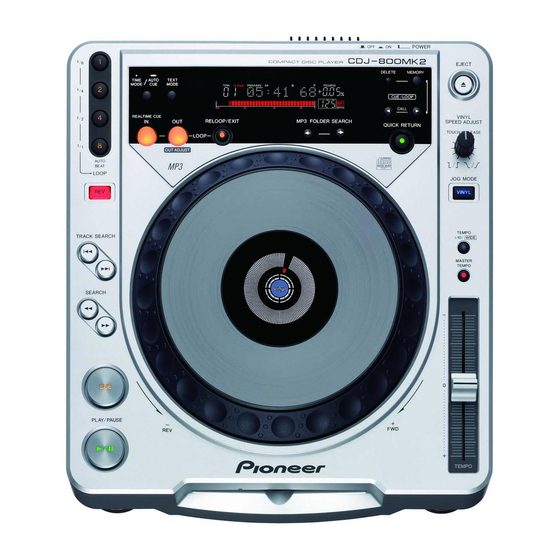
Page 140: Panel Facilities
• To set to time display, press the TIME MODE/AUTO CUE button. Back cue 6. Display Cue point sampler 7. FOLDER SEARCH buttons (← , →) 27. SEARCH buttons ( During MP3 playback, layered CD-ROM folder search will be per- formed in the designated direction. CDJ-800MK2... - Page 141 When a commercially available miniplug cord (or the accessory con- trol cord) is used to connect this jack to the same jack on another CDJ-800MK2, recorded data such as cue points and loop points can be copied from one player to the other .
-
Page 142: Display Section
This display shows the Beats-Per-Minute (BPM) of the currently play- ing track (detection range 70 to 180 BPM). The automatic BPM coun- ter may be unable to compute the correct BPM for some tracks. 63. Master tempo indicator (MT) Lights when the master tempo function is ON. CDJ-800MK2... - Page 143 CDJ-800MK2...
- Page 144 • Before shipping out the product, be sure to clean the following positions by using the prescribed cleaning tools: Position to be cleaned Position to be cleaned Cleaning tools Cleaning tools Remark Remark Pickup leneses Cleaning liquid : GEM1004 Refer to "2.4 SLOT-IN MECHANISM SECTION" , "7.1.5 DISASSEMBLY SECTION". Cleaning paper : GED-008 CDJ-800MK2...
- Page 145 PIONEER CORPORATION 4-1, Meguro 1-chome, Meguro-ku, Tokyo 153-8654, Japan PIONEER ELECTRONICS (USA) INC. P.O. Box 1760, Long Beach, CA 90801-1760, U.S.A. PIONEER EUROPE NV Haven 1087, Keetberglaan 1, 9120 Melsele, Belgium PIONEER ELECTRONICS ASIACENTRE PTE. LTD. 253 Alexandra Road, #04-01, Singapore 159936 PIONEER CORPORATION 2006 T –...
- Page 146 Ex.2 When there are 3 effective digits (such as in high precision metal film resistors). 5.62k Ω → 562 × 10 → 5621 ............RN1/4PC 5 6 2 1 CONTRAST TABLE CDJ-800MK2/WAXJ5 and CDJ-800MK2/KUCXJ are constructed the same except for the following : Part No. Ref. Mark Symbol and Description CDJ-800MK2 CDJ-800MK2 Remarks...
- Page 147 PIONEER CORPORATION 4-1, Meguro 1-chome, Meguro-ku, Tokyo 153-8654, Japan PIONEER ELECTRONICS (USA) INC. P.O. Box 1760, Long Beach, CA 90801-1760, U.S.A. PIONEER EUROPE NV Haven 1087, Keetberglaan 1, 9120 Melsele, Belgium PIONEER ELECTRONICS ASIACENTRE PTE. LTD. 253 Alexandra Road, #04-01, Singapore 159936 PIONEER CORPORATION 2002 T-ZZR OCT.
-
Page 148: Safety Precautions
The use of a substitute replacement component which does Leakage 0.5mA current Device not have the same safety characteristics as the PIONEER tester under recommended replacement one, shown in the parts list in test this Service Manual, may create shock, fire, or other hazards. - Page 149 IMPORTANT THIS PIONEER APPARATUS CONTAINS LASER DIODE CHARACTERISTICS LASER OF CLASS 1. MAXIMUM OUTPUT POWER: 5 mW SERVICING OPERATION OF THE APPARATUS WAVELENGTH: 780 – 785 nm S H O U L D B E D O N E B Y A S P E C I A L LY INSTRUCTED PERSON.
-
Page 150: Notes On Servicing
[ Important symbols for good services ] In this manual, the symbols shown-below indicate that adjustments, settings or cleaning should be made securely. When you find the procedures bearing any of the symbols, be sure to fulfill them: 1. Product safety You should conform to the regulations governing the product (safety, radio and noise, and other regulations), and should keep the safety during servicing by following the safety instructions described in this manual. - Page 151 CONTENTS SAFETY INFORMATION............................2 1. SPECIFICATIONS .............................6 2. EXPLODED VIEWS AND PARTS LIST......................8 2.1 PACKING ..............................8 2.2 EXTERIOR SECTION ..........................10 2.3 CONTROL PANEL SECTION........................12 2.4 SLOT-IN MECHANISM SECTION ......................14 3. BLOCK DIAGRAM AND SCHEMATIC DIAGRAM ..................16 3.1 BLOCK DIAGRAM............................16 3.2 OVERALL WIRING DIAGRAM .........................18 3.3 MAIN ASSY(1/2)............................20 3.4 MAIN ASSY(2/2)............................22 3.5 AC IN, TRNS, SECB and REGB ASSYS....................24...
-
Page 152: Specifications
1. SPECIFICATIONS 2. Audio section 1. General Frequency response .........4 Hz to 20 kHz System ......Compact disc digital audio system Signal-to-noise ratio ....115 dB or more (JEITA) Power requirements ......(KUCXJ)AC 120 V, 60 Hz Distortion ..........0.006% (JEITA) Power requirements ....(WYXJ)AC 220 -240V, 50/60 Hz Power consumption .......... - Page 153 CDJ-800...
-
Page 154: Exploded Views And Parts List
2. EXPLODED VIEWS AND PARTS LIST NOTES: Parts marked by "NSP" are generally unavailable because they are not in our Master Spare Parts List. mark found on some component parts indicates the importance of the safety factor of the part. Therefore, when replacing, be sure to use parts of identical designation. - Page 155 PACKING parts List Mark No. Description Part No. Mark No. Description Part No. Sheet RHX1006 > AC Power Cord See Contrast table(2) Push Rod DEX1008 Control Cord PDE-319 Audio Cord VDE1052 Pad A DHA1555 Operating Instructions See Contrast table(2) Packing Case See Contrast table(2) Polyethylene Bag Z21-038...
-
Page 156: Exterior Section
2.2 EXTERIOR SECTION Refer to "2.3 CONTROL PANEL SECTION". WYXJ type only 15 16 Refer to "2.4 SLOT-IN MECHANISM SECTION". CDJ-800... - Page 157 EXTERIOR SECTION parts List Mark No. Description Part No. Mark No. Description Part No. 25P F•F•C/60V DDD1223 MAIN Assy DWG1563 AC IN Assy See Contrast table(2) NSP 21 Silicon Rubber D5 L DEB1456 TRNS Assy DWR1364 Bottom Cushion S4 DEC2506 SECB Assy DWR1361 Bottom Plate P...
-
Page 158: Control Panel Section
2.3 CONTROL PANEL SECTION Lubricaing oil : ZLB-PN397B 13-2/2 13-1/2 CDJ-800... - Page 159 CONTROL PANEL SECTION parts List Mark No. Description Part No. MFLB Assy DWG1564 KSWB Assy DWS1321 JFLB Assy DWG1565 SLDB Assy DWS1323 JOGB Assy DWG1566 Display Panel DAH2139 RELOOP Guard DNK4057 Control Panel DNK4054 QR Guard DNK4058 Rotary Knob C DAA1143 Slide Knob DAC2067...
-
Page 160: Slot-In Mechanism Section
2.4 SLOT-IN MECHANISM SECTION Paint grease the inner surface of the wall. Grease (ZLB-PN397B) Paint on side of axle. Grease Grease (ZLB-PN397B) (ZLB-PN397B) Paint grease the inner Paint grease the inner surface of the wall. surface of the wall. Dyefree Dyefree (ZLX-ME413A) (ZLX-ME413A) - Page 161 SLOT-IN MECHANISM SECTION parts List Mark No. Description Part No. Connector Assy DKP3522 Spacer Por (T3) DEB1566 Float Base S4 Assy DXB1772 Front Sheet DED1132 Vessel Cushion A DEC2455 Vessel Cushion B DEC2456 Clamp Spring DBH1374 Guide Spring DBH1375 SW. Lever Spacer (Pet) DEC2420 Clamp Magnet DMG1009...
-
Page 162: Block Diagram And Schematic Diagram
3. BLOCK DIAGRAM AND SCHEMATIC DIAGRAM 3.1 BLOCK DIAGRAM IC109 MAIN ASSY K4S281632C-TC1H SDRAM LR Clock Audio CD MECHANISM 50MHz Data CN113 (16P) AOUT PICKUP IC118 IC102 ASSY LRCK TA2153FN PDC101A RF AMP ASIC IC110 TC9495F O_SDATA SERVO PROCESSOR 25MHz 25MHz T+,T- T+,T-... - Page 163 CN110 ONLY DESIGNER USER IC103 (1/2) NJM4558MD AUDIO IC104 PE8001A DIGITAL 16MHz MFLB ASSY 4MHz Serial data SLDB ASSY Latch clock IC502 V501 UPD16306B IC501 MAIN FL FL DRIVER PD5848A DISPLAY MICROCOMPUTER CN501 (19P) PANEL KEY CN503 CN1503 (11P) Slider (11P) CN502 CN500...
-
Page 164: Overall Wiring Diagram
3.2 OVERALL WIRING DIAGRAM SLMB ASSY (DWS1322) LOADING MOTOR ASSY-S DXX2510 CD MECHANISM (DXA-DA114) 1/2- MAIN ASSY (DWG1563) AKP7032 (KUCXJ) BKP1046 (WYXJ) AC POWER CORD (KUCXJ : ADG7021) (WYXJ : ADG1154) AC IN ASSY TRNS ASSY (KUCXJ : DWR1366) (DWR1364) (WYXJ : DWR1363) REGB ASSY... - Page 165 Note : When ordering service parts, be sure to refer to "EXPLODED VIEWS and PARTS LIST" or "PCB PARTS LIST". KSWB ASSY (DWS1321) SLDB ASSY (DWS1323) SECB ASSY (DWR1361) MFLB ASSY (DWG1564) JFLB ASSY (DWG1565) JOGB ASSY (DWG1566) CDJ-800...
-
Page 166: Main Assy(1/2)
3.3 MAIN ASSY(1/2) DSS1139 ONLY DESIGNER USER ONLY DESIGNER USER (AD) (AD) (AD) (AD) CDJ-800... - Page 167 MAIN ASSY (DWG1563) (AD) (RF) : RF SIGNAL ROUTE (AD) : AUDIO DATA SIGNAL ROUTE : DIGITAL OUT SIGNAL ROUTE : FOCUS SERVO SIGNAL ROUTE : TRACKING SERVO SIGNAL ROUTE TO CD MECHANISM CDJ-800...
-
Page 168: Main Assy(2/2)
3.4 MAIN ASSY(2/2) MAIN ASSY (DWG1563) (AD) CDJ-800... - Page 169 (AD) CN53 : AUDIO SIGNAL ROUTE (AD) : AUDIO DATA SIGNAL ROUTE : DIGITAL OUT SIGNAL ROUTE : The power supply is shown with the marked box. CDJ-800...
-
Page 170: Ac In, Trns, Secb And Regb Assys
3.5 AC IN, TRNS, SECB and REGB ASSYS TRNS ASSY (DWR1364) AC IN ASSY (KUCXJ : DWR1366) (WYXJ : DWR1363) FU11 KUCXJ: 1.6A/125V (REK1077) WYXJ: T800mA/L250V (REK1021) LIVE NEUTRAL AC POWER CORD KUCXJ: ADG7021 WYXJ: ADG1154 KUCXJ: DTT1169 WYXJ: DTT1168 •... - Page 171 SECB ASSY (DWR1361) : The power supply is shown with the marked box. REGB ASSY (DWR1362) CN1901 CDJ-800...
-
Page 172: Mflb, Slmb And Kswb Assys
3.6 MFLB, SLMB and KSWB ASSYS MFLB ASSY (DWG1564) MFLB ASSY Switches CN6001 CN56 CDJ-800... - Page 173 SLMB ASSY (DWS1322) KSWB ASSY (DWS1321) CN55 KSWB ASSY Switches S1503 : TRKB S1504 : TRKF S1501 : SCNB S1502 : SCNF S1505 : CUE S1506 : PLAY F G H : The power supply is shown with the marked box. CDJ-800...
-
Page 174: Jflb, Sldb And Jogb Assys
3.7 JFLB, SLDB and JOGB ASSYS JFLB ASSY (DWG1565) CDJ-800... - Page 175 SLDB ASSY (DWS1323) SLDB ASSY Switches S1554 : EJECT S1553 : VINYL S1552 : TEMPO S1551 : MT JOGB ASSY (DWG1566) : The power supply is shown with the marked box. I J K CDJ-800...
- Page 176 Waveforms MAIN ASSY IC118-28 pin (RFO) IC118-14 pin (TEO) IC110-12 pin (SBOK) V: 500mV/div. H: 100nS/div. V: 0.5V/div. H: 1mS/div. V: 5V/div. H: 1mS/div. • Mode: STD • Mode: SR IC118-25 pin (ARF) IC113-1 pin (T+) 905 play Single jump (reverse side only) V: 500mV/div.
- Page 177 Voltages MAIN ASSY IC110 (TC9495F-P) IC112 (PD3442A8) IC117 (XCA56367PV150) Pin No Voltage (V) Pin No Voltage (V) Pin No Voltage (V) Pin No Voltage (V) Pin No Voltage (V) Pin No Voltage (V) Pin No Voltage (V) 0-3.3 0-3.3 0-3.3 0-3.3 0-3.3 0-3.3...
- Page 178 MAIN ASSY MAIN ASSY IC109 IC118 (TA2153FN) IC119 (LA6565) IC102 (PDC101A) IC104 (PE8001A) (K4S281632C-TC1H) Pin No Voltage (V) Pin No Voltage (V) Pin No Voltage (V) Pin No Voltage (V) Pin No Voltage (V) Pin No Voltage (V) Pin No Voltage (V) 0-3.3 0-3.3...
- Page 179 MFLB ASSY JFLB ASSY IC501 (PD3848A) IC502 (UPD16306B) IC601 (UPD16306B) Pin No Voltage (V) Pin No Voltage (V) Pin No Voltage (V) Pin No Voltage (V) Pin No Voltage (V) Pin No Voltage (V) 0-42 0-31 0-42 0-31 0-42 0-31 0-42 0-31 0-42...
- Page 180 CDJ-800...
-
Page 181: Pcb Connection Diagram
4. PCB CONNECTION DIAGRAM NOTE FOR PCB DIAGRAMS : 1. Part numbers in PCB diagrams match those in the schematic 3. The parts mounted on this PCB include all necessary parts for diagrams. several destinations. 2. A comparison between the main parts of PCB and schematic For further information for respective destinations, be sure to diagrams is shown below. -
Page 182: Main Assy
4.1 MAIN ASSY SIDE A SIDE A MAIN ASSY Q108 Q105 Q107 IC103 IC107 Q104 Q106 IC111 IC115 Q103 Q102 IC123 IC104 IC118 IC125 IC108 Q111 To CD Mech anism IC117 IC110 Q110 IC113 IC114 IC102 IC112 IC109 IC119 R287 IC116 IC122 IC124... - Page 183 SIDE B SIDE B MAIN ASSY 1.F- 2.T- 3.T+ 4.F+ 5.PD 6.VR 7.LD 8.GND 10.C 11.B 14.E 12.A 15.CD+5 13.D 16.VC (DNP2035-A) CDJ-800...
-
Page 184: Ac In And Trns Assys
4.2 AC IN and TRNS ASSYS SIDE A SIDE A AC IN ASSY NEUTRAL FU101 _A_V NEUTRAL RISK OF FIRE - REPLACE AC IN FUSE DWR1359 MARKED DWR1363 /KUC/J/WY/NK LIVE DWR1365 DWR1366 LIVE POWER SW ACIN PRIMARY (DNP2036-B) TRNS ASSY CAUTION REPLACE IC LINKS... - Page 185 SIDE B SIDE B AC IN ASSY NEUTRAL NEUTRAL AC IN LIVE LIVE 2.NEUTRAL MANUAL SOLDER 1.LIVE POWER SW 3.NEUTRAL 2.220-240V ACIN 1.110-120V PRIMARY (DNP2036-B) TRNS ASSY ATTENTION REMPLACER LE IC LINKS COMME INDIQUE. DE CHEZ LITTELFUSE INC. IC23 IC24 IC25 TRNS CN22...
-
Page 186: Secb, Regb And Slmb Assys
4.3 SECB, REGB and SLMB ASSYS SIDE A SIDE A SECB ASSY REGB ASSY REGB DWR1362 JA51 1.V+7B 2.GND 3.V+5D 4.V+11B 5.V+7 6.GND (DNP2036-B) (DNP2036-B) CN51 CN22 SLMB ASSY SLOTSW SLOTSW CN1901 3.LPS2 2.GNDD 1.LPS1 (DNP2036-B) IC59 IC57 Q54 Q53 IC56 D E G CDJ-800... - Page 187 SIDE B SIDE B SECB ASSY REGB ASSY (DNP2036-B) CN51 CN22 SLMB ASSY SLOTSW SLOTSW 3.LPS2 2.GNDD 1.LPS1 (DNP2036-B) (DNP2036-B) IC59 IC57 Q54 Q53 IC56 D E G CDJ-800...
-
Page 188: Mflb And Kswb Assys
4.4 MFLB and KSWB ASSYS SIDE A MFLB ASSY D511 MFLB DWG1 W549 GLED V501 C502 Q501 D512 W540 W538 FL HOLDER S504 C506 C503 W539 D513 TIME W525 D507 D508 W524 VLDJ C510 D505 RELOOP D506 /EXIT Q502 D514 S507 S506 S505... - Page 189 SIDE A Production Code B DWG1564- W555 GNDAD MEMORY W541 S503 W544 W540 C504 W543 LDER GNDAD W542 V5AD W546 W545 S502 CALL X501 D515 S501 C509 QUICK RETURN CN1503 (DNP2036-B) (DNP2036-B) CDJ-800...
- Page 190 SIDE B MFLB ASSY MFLB DWG156 GNDAD R547 MEMORY VLDM R585 S503 GNDAD C504 V5AD R539 R531 R584 R540 R548 C539 C517 R563 R562 CALL C518 CNVSS R501 R561 XRESETM R560 S502 R559 XSRDY2 R558 SCLK21 C543 C511 QUICK C522 RETURN C509 Q503...
- Page 191 SIDE B D511 DWG1564- GLED R591 MANUAL R590 V+7B SOLDER GLED S1CK TSDI SENBL FLAC1 TSDO FLAC2 XSRST VLDM D512 VLDJ CN56 JOG1 JOG0 FLAC3 FLAC4 S504 TIME D513 C543 VLDJ Q507 Q505 Q513 S507 D514 RELOOP LOOP-OUT LOOP-IN /EXIT S505 S506 GLED...
-
Page 192: Sldb, Jogb And Jflb Assys
4.5 SLDB, JOGB and JFLB ASSYS SIDE A JFLB ASSY JFLB DWG1565- W645 DC FC W635 W622 W624 W626 C607 W621 W625 W623 CN602 W619 W620 V601 TCH1 CN601 Production code (DNP2037-B) SLDB ASSY S1551 SLDB DWS1323- D1553 VR1551 W608 CDJ-800... - Page 193 SIDE A JOGB ASSY (DNP2037-B) CN503 CN1503 CN1503 W617 GNDF W616 W610 GNDF ADIN W609 S1551 D1552 S1552 ADCT W613 D1553 V5AD W612 W618 D1551 GNDF GNDAD S1554 W607 VR1552 (DNP2037-B) CDJ-800...
- Page 194 SIDE B JFLB ASSY JFLB DWG1565- Q608 C604 C601 CN600 1.FLAC4 FLAC4 FLAC3 JOG0 JOG1 VLDJ SCLK2 SDO2 LATCH1 13.BLK1 C602 VLDJ C607 Q603 Q606 VLDJ Q605 VLDJ CN602 C603 TCH1 CN601 TCH1 CN601 (DNP2037-B) IC601 Q608 Q602 Q601 IC602 Q606 Q607 Q605 Q603 Q604...
- Page 195 SIDE B JOGB ASSY C1602 D1601 R1603 C1601 R1602 JOGB R1601 DWG1566- (DNP2037-B) WARNING VR1551 ADCT THIS PRODUCT CONTAINS LEAD IN SOLDER AND CERTAIN V5AD ADCT ELECTRICAL PARTS CONTAIN CHEMICALS WHICH ARE KNOWN TO THE STATE OF CALIFORNIA TO CAUSE CANCER,BIRTH DEFECTS OR OTHER REPRODUCTIVE HARM.
-
Page 196: Pcb Parts List
5. PCB PARTS LIST NOTES: Parts marked by "NSP" are generally unavailable because they are not in our Master Spare Parts List. mark found on some component parts indicates the importance of the safety factor of the part. Therefore, when replacing, be sure to use parts of identical designation. When ordering resistors, first convert resistance values into code form as shown in the following examples. -
Page 197: Mflb Assy
Mark No. Description Part No. Mark No. Description Part No. C253, C267-C269, C273, C280 CKSRYB104K25 S501, S502, S503, S504 ASG7013 C285-C287, C291 CKSRYB104K25 S505, S506, S507, S508 DSG1063 S509, S510, S511, S512 DSG1063 C195 CKSRYB153K50 C197, C203, C228, C229, C279 CKSRYB224K16 CAPACITORS C204... - Page 198 Mark No. Description Part No. Mark No. Description Part No. C53, C54 CEAT332M16 COILS AND FILTERS CKSRYB103K50 > VTL-004 C56, C63, C66 CKSRYB104K25 SWITCHES AND RELAYS RESISTORS > DSA1029 RD1/2VM103J RD1/2VM271J CAPACITORS RD1/2VM470J > C12, C13 (Film capa.) ACE7027 RS1/16S2002D >...
- Page 199 Mark No. Description Part No. C609, C610, C611, C612, C613 CKSRYB103K50 C615 CKSRYB103K50 RESISTORS Other Resistors RS1/16S###J OTHERS CN602 CONNECTOR 5597-03APB V601 FL DISPLAY DEL1049 FL HOLDER DNK3956 CN600 13P CONNECTOR HLEM13R-1 CN601 KR CONNECTOR S4B-PH-K-S SLMB ASSY SWITCHES AND RELAYS S1901, S1902 DSG1017 OTHERS...
-
Page 200: Adjustment
6. ADJUSTMENT There is no information to be shown in this chapter. CDJ-800... -
Page 201: General Information
7. GENERAL INFORMATION 7.1 DIAGNOSIS 7.1.1 SERVICE MODE 1. Service Mode Summary This unit is controlled with two microcomputers. One microcomputer performs the button input and indication of FL and LED (display section), and the other microcomputer drives the player (player section). Test mode is prepared in each microcomputer. - Page 202 3. Confirmation Mode of the Operation with the Player being Simple Connect the remote control unit (RU-V101) to DATA IN/OUT terminal of the Rear panel, and confirms the operation. These commands test a mechanism and servo system mainly. Therefore, DJ function such as scan or tempo does not work. Prepare only a command that searches arbitrary music and playback the audio.
- Page 203 (Pause) Pauses at the position. (Eject) In the playback state or stop state, perform the disc eject. (Audio Play) Audio playbacks the arbitrary music. It is necessary for this command that Player is set up beforehand. Please execute (Play) first. (Reject) Stop by the command.
- Page 204 4. Version confirmation mode Confirm the software version of each microcomputer. • Symptom of the microcomputer software version of the display section Turn the power on while pressing the [MEMORY] and [TRACK-SEARCH-REV] buttons, then two figures character is displayed at the track number display section. This shows a version. (First edition is as 10) •...
- Page 205 Chart of a remote control unit function of CDJ-800 * Caution in the remote control unit use: Please connect to the DATA IN/OUT terminal before turning the power on. REJECT PAUSE PLAY Stop Pause Play STILL/STEP Invalidity – MULTI-SPEED + Invalidity SCAN Invalidity...
-
Page 206: Power On Sequence
7.1.2 POWER ON SEQUENCE Power ON IC112 (System Control CPU) Reset release pin 63 IC102 (ASIC) Reset release pin 91: H IC501 (Display CPU) Reset release pin 18: H IC117 (Audio DSP) Reset release pin 44: H IC110 (Servo DSP) Reset release pin 100: H IC117 (Audio DSP) Program download Tracking and focus offset adjustment Spindle extra kick... - Page 207 GOOD OR BAD JUDGEMENT METHOD OF THE PICKUP 1. LD current : 20 to 80mA TYP : 40 to 50mA Measure both end of R249 on the MAIN Assy in the play state. (Fig. 1) There must be the value that divided the measured value with 23.5 Ω within the numerical value mentioned above. 2.
-
Page 208: Disassembly
7.1.3 DISASSEMBLY MAIN Assy CD Mechanism Remove three screws to remove the Bottom Plate M. Remove three screws to remove the Bottom Plate M. Remove four screws to remove the Bottom Plate P. Bottom Plate M Short land Remove a screw. Bottom View Remove four screws. - Page 209 Control Panel Section JOG Section Remove five screws. Release a Cord Clamper. Disconnect a flexible cable. Remove six screws. CN500 Bottom View Bottom View Unhook three hooks. Remove the JOG B and JOG A. Remove a screw. Rear View JOG A JOG B Remove the Control Panel Section.
- Page 210 Caution in Sheet SW Installation Caution in Roller A Assy Installation Be careful not to bend and fold the Sheet SW. Apply a grease to the shaft bearing section of JOG Holder side and SW Ring side. Confirm that the dust or trash does not adhere to pasting side (Apply it to two places for roller one.) (JOG Holder).
-
Page 211: Parts
7.2 PARTS 7.2.1 IC • The information shown in the list is basic information and may not correspond exactly to that shown in the schematic diagrams. ÷ List of IC PD3442B8, PD101A, NJM2374AM, NJM2870F05 PD3442B8 (MAIN ASSY : IC112) • SYSTEM CONTROL Microcomputer ÷... - Page 212 • Pin Function µ t i c t i r l a i l a i l l o l a i l a i l l o l l o n i l CDJ-800...
- Page 213 • Pin Function i g i l l i CDJ-800...
- Page 214 • Pin Function d i l d i l c t i CDJ-800...
- Page 215 PD101A (MAIN ASSY : IC102) ASIC Microcomputer • ÷ Pin Function(1/4) / I ( / I ( / I ( CDJ-800...
- Page 216 • Pin Function(2/4) / I ( / I ( / I ( GND f CDJ-800...
- Page 217 • Pin Function(3/4) c t i c t i c t i / I ( c t i c t i c t i c t i / I ( / I ( CDJ-800...
- Page 218 • Pin Function (4/4) / I ( / I ( CDJ-800...
- Page 219 7 NJM2374AM (MAIN ASSY : IC107) ÷ DC-DC CONVERTER ÷ Block Diagram 1 . Cs 2 . Es 3 . Cr 4 . GND 5 . IN 6 . V 7 . S 8 . Cp ÷ Pin Arrangement CDJ-800...
- Page 220 7 NJM2870F05 (MAIN ASSY : IC123) ÷ 5V Regulator ÷ Pin Configuration PIN FUNCTION 1 . CONTROL 2 . GND 3 . NOISE BYPASS 4 . Vout 5 . Vin ÷ Block Diagram CDJ-800...
-
Page 221: Display
7.2.2 DISPLAY DEL1048 (MFLB ASSY : V501) • FL Indicator Tube Grid Assignment Pin Connection Anode Connection CDJ-800... -
Page 222: Panel Facilities
8. PANEL FACILITIES 8.1 PANEL FACILITES 7 Front Panel 2 3 4 5 8 9 10 2 DIGITAL OUT MODE switch (DJ/NORMAL) 1. TIME MODE/AUTO CUE button (*) This switch is located on the unit's rear panel. TIME MODE: When set to DJ, the DIGITAL OUT connector Each time this button is pressed, the time display changes outputs audi odata alone. - Page 223 5 RELOOP/EXIT button (*) 16 TEMPO control slider (*) 6 Display Slide the knob towards you (+) to increase the tempo and 7 POWER switch (OFF—/ON _) slide it away from you (-) to decrease it. This switch is located on the rear panel of the unit. 17 Jog Dial Display 8 CUE/LOOP MEMORY button (*) 18 Jog dial (+FWD/-REV) (*)
-
Page 224: Jog Dial Display
7 DisPlay 51 TRACK number display Displays TRACK numbers. 60 Playback address display 52 Auto cue indicator (A. CUE) Indicates elapsed playback time and remaining playback Lights when auto cue is on. time in an easy to grasp 1-track full scale bar graph. 53 QUICK RETURN indicator ÷... - Page 225 PIONEER CORPORATION 4-1, Meguro 1-chome, Meguro-ku, Tokyo 153-8654, Japan PIONEER ELECTRONICS (USA) INC. P.O. Box 1760, Long Beach, CA 90801-1760, U.S.A. PIONEER EUROPE NV Haven 1087, Keetberglaan 1, 9120 Melsele, Belgium PIONEER ELECTRONICS ASIACENTRE PTE. LTD. 253 Alexandra Road, #04-01, Singapore 159936 PIONEER CORPORATION 2006 T –...
- Page 226 If you are not qualified to perform the repair of this product properly and safely, you should not risk trying to do so and refer the repair to a qualified service technician. IMPORTANT THIS PIONEER APPARATUS CONTAINS LASER OF CLASS 1. SERVICING OPERATION OF THE APPARATUS S H O U L D B E D O N E B Y A S P E C I A L LY INSTRUCTED PERSON.
- Page 227 Ex.2 When there are 3 effective digits (such as in high precision metal film resistors). 5.62k Ω → 562 × 10 → 5621 ............RN1/4PC 5 6 2 1 CONTRAST TABLE CDJ-800MK2/NKXJ and CDJ-800MK2/KUCXJ are constructed the same except for the following : Part No. Ref. Mark Symbol and Description CDJ-800MK2 CDJ-800MK2 Remarks...
- Page 228 Symbol and Description Remarks DWR1430 DWR1429 AC Inlet 1P XKP3042 XKP3041 DFLB ASSY DWG1646 and DWG1623 are constructed the same except for the following : Part No. Mark Symbol and Description Remarks DWG1623 DWG1646 R573, R574, R575 RS1/16S561J RS1/16S271J CDJ-800MK2...