Table of Contents
Advertisement
Quick Links
Download this manual
See also:
User Manual
Micro System
Service
Service
Service
Service
Service
Service Manual
©
Copyright 2004 Philips Consumer Electronics B.V. Eindhoven, The Netherlands
All rights reserved. No part of this publication may be reproduced, stored in a retrieval system or
transmitted, in any form or by any means, electronic, mechanical, photocopying, or otherwise
without the prior permission of Philips.
Published by BB 0411 Service Audio
Version 1.0
TABLE OF CONTENTS
Location Of Pc Boards & Version variations ................ 1-2
Technical Specifications ............................................. 1-3
Measurement Setup .................................................... 1-4
Service Aids, Safety Instruction, etc. .......................... 1-5
Disassembly Instructions & Service positions .............. 2
Service Test Program ................................................. 3-1
Set Block Diagram ...................................................... 4-1
Set Wiring Diagram ..................................................... 5-1
Front Board .................................................................... 6
ECO6 Tuner Board : Systems Non-Cenelec ............. 7A
Systems Cenelec ..................... 7B
Mains Board ................................................................... 8
Etf8 Tape Module ........................................................ 9
Universal Loader ......................................................... 10
Combi & Regulator Boards .......................................... 11
Set Mechanical Exploded View & parts list ................. 12
Printed in The Netherlands
Subject to modification
MCM7/
Page
CLASS 1
LASER PRODUCT
GB
22/37
3139 785 30610
Advertisement
Table of Contents

Related Manuals for Philips MCM7/22


Summary of Contents for Philips MCM7/22
- Page 1 LASER PRODUCT © Copyright 2004 Philips Consumer Electronics B.V. Eindhoven, The Netherlands All rights reserved. No part of this publication may be reproduced, stored in a retrieval system or transmitted, in any form or by any means, electronic, mechanical, photocopying, or otherwise without the prior permission of Philips.
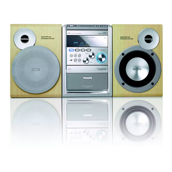
- Page 2 LOCATION OF PC BOARDS ETF8 SD Board Display Board Tuner Board Eeprom Board Regulator Board (Below Tuner Board) Mains Board CD Board MP3 CD03 Board Top Key Board Control Board Combi Board Tray Motor Board VERSION VARIATIONS: Type /Versions: MCM7 Features &...
- Page 3 SPECIFICATIONS Input sensitivity GENERAL: Aux in (at 1kHz) : 500mV at 600 ohm Mains voltage : 110-127V/220-240V Switchable for /21/21M CDR in (at 1kHz) : 1000mV at 600 ohm 120V for /37 220V for /33 Output sensitivity 220-230V for /22 Headphone output at 32 ohm : 15mW ±...
-
Page 4: Measurement Setup
MEASUREMENT SETUP Tuner FM Bandpass LF Voltmeter 250Hz-15kHz e.g. PM2534 e.g. 7122 707 48001 RF Generator e.g. PM5326 S/N and distortion meter e.g. Sound Technology ST1700B Use a bandpass filter to eliminate hum (50Hz, 100Hz) and disturbance from the pilottone (19kHz, 38kHz). Tuner AM (MW,LW) Bandpass LF Voltmeter... -
Page 5: Service Aids
SERVICE AIDS Service Tools: Universal Torx driver holder ........4822 395 91019 Torx bit T10 150mm ..........4822 395 50456 Torx driver set T6 - T20 ......... 4822 395 50145 Torx driver T10 extended ........4822 395 50423 Compact Disc: SBC426/426A Test disc 5 + 5A ...... - Page 6 WAARSCHUWING WARNING Alle IC’s en vele andere halfgeleiders zijn All ICs and many other semi-conductors are gevoelig voor electrostatische ontladingen (ESD). susceptible to electrostatic discharges (ESD). Onzorgvuldig behandelen tijdens reparatie kan Careless handling during repair can reduce life de levensduur drastisch doen verminderen. drastically.
- Page 7 DISMANTLING INSTRUCTIONS Dismantling of the Cover Cassette and Universal Loader Detaching the Universal Loader from the Bracket Module Mounting 1) Remove the Cover Cassette (pos 150) in the direction as 1) Slide out the Loader Tray fully and remove 4 screws B (see shown in Figure 1.
- Page 8 DISMANTLING INSTRUCTIONS Dismantling of the Front Panel assembly Dismantling of the Front Panel assembly 1) The Knob Volume (pos 141) can be remove by pulling it 5) Loosen 1 screw F and 4 catches C3 (see Figure 11) to out in the direction as shown in Figure 8. remove the Eeprom Board (pos 1105D).
- Page 9 DISMANTLING INSTRUCTIONS Repair Hints & Service Positions Service position B 1) During repair it is possible to disconnect the Tuner Board Note: The flex cables are very fragile, care should be taken and/or CD Module completely unless the fault is sus- not to damage them during repair.
- Page 10 SERVICE TEST PROGRAM To start service test program hold & ECO depressed while plugging in the mains cord S refers to Service Mode Display shows the ROM version V refers to Version "S-Vyy" yy refers to Software version number of the uProcessor (Main menu) (counting up from 01 to 99) QUARTZ...
- Page 11 SET BLOCK DIAGRAM +12V_M -6dB Track NOTE : +12V_A MAIN SIGNAL PATH UL-ICD03 285mV 125mV MEASUREMENTS ARE IN AUX MODE : FM (67.5 kHz) ECO6 AM (80% MOD) XX mV LEVELS AT MAX VOL YY dBA S/N AT 500mW CONTROL ZZ dB HEADROOM (1% THD) WRT TO LEVEL AT MAX VOL TUNER...
- Page 12 SET WIRING DIAGRAM 8008 BI 8008 EHT 1404 3P/180mm FCS 1402 FCT 1025 FCT 1018 FCS 1801 FCS 1803 FCS 1451 8006 3139 110 36001 TOP KEY 9P/180mm/AD 8003 (CDC KEY) FRONT 15P/280mm/BD/Fold (1105) 3139 110 35081 DISPLAY 8004 3139 111 03871 19P/98mm/BD EEPROM (1105)
- Page 13 TECHNICAL REMARKS FRONT BOARD TABLE OF CONTENTS FTD Display Pin Connection ........... 6-2 Display part - Component Layout ........6-3 Display part - Chip Layout ..........6-4 Display part - Circuit Diagram Part 1 ......6-5 Display part - Circuit Diagram Part 2 ......6-6 Display part - Variant Table ..........
-
Page 14: Ftd Display Pin Connection
FTD DISPLAY PIN CONNECTION B2 B3 B4 B5 B6 B7 C1 C2 C3 C4 C5 C5 C6 C6 C7 (1G) (13G) (1G) (12G) (2G - 11G) j , p j , p j , p j , p j , p j , p j , p j , p... - Page 15 DISPLAY BOARD - COMPONENT LAYOUT This assembly drawing shows a summary of all possible versions. For components used in a specific version see schematic diagram and respective parts list. 3139 113 3529 pt4 dd wk0409...
- Page 16 DISPLAY BOARD - CHIP LAYOUT This assembly drawing shows a summary of all possible versions. For components used in a specific version see schematic diagram and respective parts list. 3139 113 3529 pt4 dd wk0409...
- Page 17 DISPLAY BOARD - CIRCUIT DIAGRAM PART 1 1400 A13 3473 C7 1404 C1 3474 C7 1405 E1 3475 C7 1406 E13 3476 C7 1407 G13 3477 C7 2400 H12 3478 C6 2401 H1 3479 C6 7406 BC847B 2402 H2 3480 C6 Note : Some values may varies, see respective parts list for correct value.
- Page 18 DISPLAY BOARD - CIRCUIT DIAGRAM PART 2 1401 A3 2442 C6 2446 D4 2450 F3 2454 F3 2460 C9 2464 F10 2468 F10 2472 C9 3501 B5 3505 D4 3509 B8 3513 B10 3517 C8 3521 F9 3525 D6 4408 C4 4413 E6 4422 C5 4427 C5...
- Page 19 DISPLAY BOARD - VARIANT TABLE TOP KEY BOARD - COMPONENT LAYOUT This assembly drawing shows a summary of all possible versions. For components used in a specific version see schematic diagram and respective parts list. MCM7/22 MCM7/37 MCM8/22 MCM8/21 2444...
- Page 20 CONTROL BOARD - COMPONENT LAYOUT This assembly drawing shows a summary of all possible versions. For components used in a specific version see schematic diagram and respective parts list. 3139 113 3529 pt4 dd wk0409 CONTROL BOARD - CHIP LAYOUT This assembly drawing shows a summary of all possible versions.
- Page 21 CONTROL BOARD - CIRCUIT DIAGRAM PART 1 1300 A7 1302 A1 1304 A5 1306 A6 1308 A4 1310 A3 1312 E2 1314 E5 2301 A8 2304 E2 2306 E3 2308 E5 2310 E6 3302 A3 3304 A4 3306 A5 3308 A5 3313 D3 3315 D5 3317 D6...
- Page 22 6-10 6-10 CONTROL BOARD - CIRCUIT DIAGRAM PART 2 2303 D5 2312 A4 2314 C3 2316 C8 3319 C2 3321 D2 3323 B5 3325 B6 3327 B7 3329 B7 3331 B8 3333 B9 3335 D5 5303 A3 6300 B8 6302 B6 6304 B8 6309 C5 7302 C9...
- Page 23 6-11 6-11 EEPROM BOARD - COMPONENT LAYOUT EEPROM BOARD - CIRCUIT DIAGRAM 1600 A4 2601 C1 2603 D1 2605 D4 2607 E3 3601 B2 3603 C1 3605 E2 3607 D3 5601 C2 7600 A1 2600 A2 2602 D1 2604 D3 2606 E2 3600 B2 3602 C1...
- Page 24 6-12 6-12 KARAOKE BOARD - COMPONENT LAYOUT (For MCD9 only) KARAOKE BOARD - CHIP LAYOUT (For MCD9 only) This assembly drawing shows a summary of all possible versions. This assembly drawing shows a summary of all possible versions. For components used in a specific version see schematic diagram and respective parts list. For components used in a specific version see schematic diagram and respective parts list.
- Page 25 6-13 6-13 KARAOKE BOARD - CIRCUIT DIAGRAM (For MCD9 only) 1800 B1 2801 C7 2804 B6 2807 C4 2810 B3 2813 D5 2816 E3 2819 E6 3802 A3 3805 C7 3808 B6 3811 B4 3814 A2 3817 D4 3820 D3 3823 E7 6800 D3 7800-B B7...
-
Page 26: Front Board
6-14 6-14 ELECTRICAL PARTS LIST - FRONT BOARD ELECTRICAL PARTS LIST - FRONT BOARD MISCELLANEOUS 1300 4822 265 11183 Flex Connector 4P 2411 4822 122 33761 22pF 5% 50V 3326 4822 051 30152 1k5 5% 0,062W 3441 4822 051 30102 1k 5% 0,062W 1301 2422 026 05563... - Page 27 6-15 6-15 ELECTRICAL PARTS LIST - FRONT BOARD ELECTRICAL PARTS LIST - FRONT BOARD RESISTORS 3496 4822 051 30103 10k 5% 0,062W 4411 4822 051 30008 0R Jumper 0603 5602 4822 242 11033 RES XTL 4,332MHz /22 3497 4822 050 21003 10k 1% 0,6W 4420 4822 051 30008...
- Page 28 7A-1 7A-1 BLOCK DIAGRAM TUNER BOARD ECO 6 Systems Vcc1 buffer ampl. Stab Stab Discriminator FM-RF FM-IF 1 FM-IF 2 (MPX) Vcc2 1101 Loop (1102) LF filter 10,7 MHz 10,7 MHz 10,7 MHz 1120 left left Stereo right right Det. Decoder Frontend Mixer...
- Page 29 7A-2 7A-2 1101 A1 1102 B1 1103 F2 1120 E14 1130 A2 TUNER BOARD ECO6 1131 B2 / SYSTEMS NON CENELEC 1132 G13 2101 B3 VERSION PROGRAMMING COMPONENTS 2102 B1 1101 2103 C7 2105 2104 B3 AM-IF1 1130 2105 A2 100n 5111 450kHz...
- Page 30 7A-3 7A-3 1101 A6 1120 A4 1132 A5 2128 C4 2138 C2 3142 D2 5110 B3 5114 A2 5123 D5 7112 C1 9104 B5 9107 D4 TUNER ADJUSTMENT TABLE ( ECO6 FM/MW- and FM/MW/LW - versions with AM-frame aerial ) 1102 B6 1130 B5 2106 C5...
- Page 31 7A-4 7A-4 Electrical Partslist ECO6 SYSTEMS NON CENELEC MISCELLANEOUS RESISTORS ––––––––––––––––––––––––––––––––––––––––––––––––––––– ––––––––––––––––––––––––––––––––––––––––––––––––––––– 1101 2422 015 19376 SOCKET 2P CLICKFIT 3143 © 4822 051 20223 22kΩ 0,1W USA only RDS only 1102 4822 267 10283 SOCKET COAX, IEC 75Ω 3144 © 4822 051 10102 1kΩ...
-
Page 32: Table Of Contents
7B-1 7B-1 BLOCK DIAGRAM AM/FM ECO6 Tuner Board SYSTEMS CENELEC version: TABLE OF CONTENTS Blockdiagram..............7B-1 varicap Schematic Diagram............7B-2 Component Layout ............7B-3 Adjustment table .............7B-3 Electrical Partslist............7B-4... - Page 33 7B-2 7B-2 1101 A2 5121 E11 1102 B1 5122 H5 1103 E2 5123 G5 1110 B2 6105-1 E4 VERSION PROGRAMMING COMPONENTS 1120 E14 6105-2 G6 TUNER BOARD ECO6 1130 A2 6106 D4 / SYSTEMS-CENELEC 1131 C2 6107 G13 VERSION AM-IF1 1132 F13 6120 C13 6120...
- Page 34 7B-3 7B-3 1101 B5 1110 B4 1131 C5 2107 B3 2133 C1 2162 A4 5102 C4 5110 A2 5114 A2 5121 B2 7104 C4 9101 A2 9104 B1 9107 B4 9110 A4 TUNER ADJUSTMENT TABLE ( ECO6 Cenelec FM/MW - and FM/MW/LW - versions with AM-frame aerial ) 1102 B5 1120 A4 1132 A4...
- Page 35 7B-4 7B-4 Electrical Partslist ECO6 SYSTEMS CENELEC MISCELLANEOUS RESISTORS DIODES ––––––––––––––––––––––––––––––––––––––––––––––––––––– ––––––––––––––––––––––––––––––––––––––––––––––––––––– ––––––––––––––––––––––––––––––––––––––––––––––––––––– 1101 2422 015 19376 SOCKET CLICKFIT 2P 3128 © 4822 117 11449 2,2kΩ 0,1W 6105 © 4822 130 83075 HN1V02H USA only LW only 1102 4822 267 10283 SOCKET COAX, IEC 75Ω...
- Page 36 Brief introduction of the Mains Board ECO Power Standby Transformer 5203 provides the LPS supply to control the relay 1210, cutting of the Mains supply to the Mains transformer during the ECO Power (standby) mode. The Mains transformer provides the following: 5V6_ECO for Low Power Supply +A, +A/2 and +B to the Combi board MAINS BOARD...
- Page 37 MAINS BOARD - COMPONENT LAYOUT This assembly drawing shows a summary of all possible versions. For components used in a specific version see schematic diagram and respective parts list. 3139 113 3478 pt3 dd wk0247...
- Page 38 MAINS BOARD - CHIP LAYOUT This assembly drawing shows a summary of all possible versions. For components used in a specific version see schematic diagram and respective parts list. 3139 113 3478 pt3 dd wk0247...
- Page 39 MAINS BOARD - CIRCUIT DIAGRAM 0003 A10 6219 F1 1200 A7 6220 D5 6221 D5 1202 B4 1203 A9 6222 C5 1205 A7 6223 C5 1206 A3 6224 E6 /37 ONLY 1207 B7 6225 E5 9250 9206 1208 B4 6226 F5 1200 1209 E10 6227 F3...
- Page 40 ELECTRICAL PARTS LIST - MAINS BOARD MISCELLANEOUS 1200 2422 086 10963 Fuse RAD LT 5A 250V 3223 4822 051 30103 10k 5% 0,062W 1202 4822 071 51252 Fuse RAD LT 1,25A 250V/22 3224 4822 117 13632 100k 1% 0,62W 1202 4822 252 51121 Fuse RAD LT 3,15A 250V/37 3225...
- Page 41 ELECTRICAL PARTS LIST - MAINS BOARD TRANSISTORS & INTEGRATED CIRCUITS 7202 4822 130 42804 BC817-25 7203 4822 130 40855 BC337-40 7204 4822 130 60373 BC857B 7205 5322 130 60159 BC847B 7206 4822 130 60373 BC857B Note : Only the parts mentioned in this list are normal service spare parts.
-
Page 42: Etf8 Tape Module
CONNECTORS ASSIGNMENTS: CONNECTOR 1701 INTERCONNECTION TO AF BOARD REC-L Record input left REC-R Record input right GND A AF Ground TAPE-L Playback output left +12V D.C. supply (+12V) for AF electronics TAPE-R Playback output right -CMOS Negative d.c. supply (-9V) for controlling JFET J111 ETF8 TAPE MODULE CONNECTOR 1703 INTERCONNECTION TO AF BOARD... - Page 43 TAPE DECK WIRING TAPE MECHANISM ELECTRONICS To ETF8 Board Connector 1760 (8P) 08FESTVKNA Motor Pin No. 1. Vcc 12V 2. Photo Out 3. Gnd Photo Interrupter 4. Mode Switch Mode Switch 5. Solenoid 6. CrO2 Switch CrO2 Switch 7. Rec Switch (FWD) Rec Switch (FWD) 8.
- Page 44 TAPE ADJUSTMENT & CHECK TABLE HEF4094BT FUNCTIONAL BLOCK DIAGRAM ADJUST TEST RECORDER MEASURE READ ON CASSETTE MODE with SBC420 frequency MOTOR SPEED PLAY check 3150Hz +/- 2% counter 3150Hz 8-STAGE SHIFT ’ SBC420 WOW & FLUTTER check PLAY W&F-meter < 0.4 % DIN REGISTER 3150Hz PLAY FWD...
- Page 45 COMPONENT LAYOUT CHIP LAYOUT This assembly drawing shows a summary of all possible versions. For components used in a specific version see schematic and respecive parts list. This assembly drawing shows a summary of all possible versions. For components used in a specific version see schematic and respecive parts list. 3139 113 3455 pt3 dd wk411 3139 113 3455 pt3 dd wk411...
- Page 46 CIRCUIT DIAGRAM 1701 D14 3786 I5 1703 A1 3789 I4 1706 A1 3790 D9 1710 F1 3791 G9 1760 A14 3792 F6 7612 +MOTOR 2621 A3 3793 F5 EH-B 1703 PMBT 2907 11.8V 2622 A3 3794 F5 +MOTOR 11.9V 2623 A3 3795 F5 11.9 +MOTOR...
- Page 47 AUTOREVERSE (AR) TAPE MECHANISM MECHANICAL PARTS LIST - AUTOREVERSE TAPE MECHANISM 9965 000 10041 Rec/Pb Head assembly 9965 000 10042 Cap Pinch R 9965 000 10043 Cap Pinch L 9965 000 10044 Roller Pinch 9965 000 10045 Solenoid assembly 9965 000 10046 Motor Assembly 9965 000 07441 Belt-SR...
- Page 48 NON-AUTOREVERSE (NAR) TAPE MECHANISM MECHANICAL PARTS LIST - NON-AUTOREVERSE TAPE MECHANISM 9965 000 12110 Play Head 9965 000 02600 Erase Head 9965 000 10042 Cap Pinch Roller 9965 000 10044 Roller Pinch 9965 000 07439 Solenoid Assy 9965 000 10046 Assembly Motor 9965 000 12114 Belt SF...
- Page 49 TAPE MODULE EXPLODED VIEW ELECTRICAL PARTS LIST - ETF8 BOARD MISCELLANEOUS 1701 4822 267 10953 Flex Socket 7pin Vert. 2732 4822 126 14043 1uF +80/-20% 16V 1706 4822 267 10953 Flex Socket 7pin Vert. 2743 4822 126 14494 22nF 10% 25V 1710 4822 267 10958 Flex Socket 5pin Hort.
- Page 50 ELECTRICAL PARTS LIST - ETF8 BOARD ELECTRICAL PARTS LIST - ETF8 BOARD RESISTORS 3710 4822 051 30339 33R 5% 0,062W 3780 4822 051 30105 1M 5% 0,062W 6771 4822 130 30621 1N4148 3711 4822 051 30101 100R 5% 0,062W 3780 4822 051 20105 1M 5% 0,1W 6772...
-
Page 51: Universal Loader
10-1 10-1 Service hints In case of symptom „skipping tracks“ perform 3. MEASURE THE LASER CURRENT following actions: CD DRIVE – LASER CURRENT MEASUREMENT 1. VERIFY THE COMPLAINT The laser current can be measured as a voltage drop on resistor 3822. Typical value 50mV (MCD2 disc drive) res- PLAYABILITY CHECK pectively 55mV (DA12 disc drive). - Page 52 10-2 10-2 Service hints Service hints CAUTION Dismantling of Drawer CHARGED CAPACITORS ON THE SERVO BOARD MAY DAMAGE THE CD DRIVE ELECTRONICS WHEN CONNECTING A NEW CD MECHANISM. THAT´S WHY, BESIDES THE SAFETY MEASURES LIKE 1. Open the drawer and release 2 catches •...
- Page 53 10-3 10-3 Abbreviations SIGNAL PROCESSOR (CD18) SAA7825 SYMBOL DESCRIPTION SYMBOL DESCRIPTION LFPOWER laser power supply digital supply voltage 1 DDD1 EXFILTER 10 nF capacitor for laser start-up control serial data input (loopback) MONITOR laser monitor diode WCLI word clock input (loopback) SENSE OPU ground reference point for MONITOR measurement SCLI...
- Page 54 10-4 10-4 BLOCK DIAGRAM Universal Loader / ICD03 PhonIC MP3 CD MAIN BOARD MM1469 7801 21, 22 +3,3V CD MECHANISM + ANALOG MCD2, DA12 +3,3V +1,8V VAM2201 DISC Active low pass Filter 7800 1800 OSC OUT to Combi Board TURNTABLE LM358 7804 8.46 MHz...
- Page 55 10-5 10-5 TRAY MOTOR BOARD / copper side view 1810 H2 1811 F3 2814 B2 2820 A2 1810 C1 2814 C3 2830 A4 3812 B2 3814 C3 3816 B2 3830 A4 3832 A3 7810 B4 F811 C2 F816 C2 F830 A5 2830 G1 1811 C2 2820 B3...
- Page 56 10-6 10-6 1800 D2 7801 G2 1801 G14 7802 I5 1803 B14 7804-1 A5 1805 H11 7804-2 A3 1810 B6 7806 G5 CD MAIN BOARD 2842 2801 A9 7807 H5 +3.3V 2802 B2 7808 H5 ICD03 / MP3 version 220p 2803 A9 F801 B3 3867...
- Page 57 10-7 10-7 WIRED COMPONENTS SURFACE MOUNTED COMPONENTS 1800 C2 CD BOARD / copper side view 1801 A4 (Universal Loader PhonIC) 1803 C5 1805 B5 1810 D3 2802 B5 2803 D4 Slide Motor 2804 B5 2809 D4 2819 D3 2828 B3 2831 B4 7802 B2 9801 B5...
- Page 58 10-8 10-8 Exploded view U NIVERSAL OADER MOTOR BOARD MECHANICAL PARTS ––––––––––––––––––––––––––––––––––––––––––––––––––––– 3103 304 71780 DRAWER 3103 304 71800 SLIDER 3103 304 71820 PULLEY GEARWHEEL 3103 304 71830 GEARWHEEL 3103 304 71910 DRIVING BELT 3103 308 54160 MOTOR ASSY 3103 301 06660 SPRING SUPPORT 3103 304 71790 SUPPORT CD...
- Page 59 10-9 10-9 ELECTRICAL PARTSLIST Universal Loader / ICD03 PhonIC MP3 Version ELECTRICAL PARTSLIST Universal Loader / ICD03 PhonIC MP3 Version –––––––––––––––––––––––––––––––––––––––––––––––––––––––––––––––––––––––––––––––––––––––––––––––––––––––––––––––––– –––––––––––––––––––––––––––––––––––––––––––––––––––––––––––––––––––––––––––––––––––––––––––––––––––––––––––––––––– MOTOR BOARD CD BOARD RESISTORS RESISTORS ––––––––––––––––––––––––––––––––––––––––––––––––––––– ––––––––––––––––––––––––––––––––––––––––––––––––––––– 3823 © 4822 051 30102 1kΩ 0,06W 4843 © 4822 051 20008 CHIP JUMPER 0805 MISCELLANEOUS MISCELLANEOUS...
- Page 60 10-10 10-10 MP3 BOARD FOR ORIENTATION ONLY 1451 F14 F406 E8 1455 B14 F407 E8 1460 F9 F408 F8 1465 A14 F409 F13 MP3 CD 2003 Board (flash version) 2450 A1 F410 F8 2451 B5 F411 E13 2452 B2 F412 G1 only for FLASH version 2453 B4 F413 G13...
- Page 61 10-11 10-11 MP3 BOARD FOR ORIENTATION ONLY MP3 CD03 Board SIDE A (flash version) MP3 CD03 Board SIDE B (flash version) MP3 CD03 flash version, 040304 1460 B3 3456 B1 3464 C3 3486 C2 3494 A1 5450 D3 7456 C2 1451 B5 2454 B2 2465 D4...
- Page 62 10-12 10-12 PERSONAL NOTES:...
-
Page 63: Combi & Regulator Boards
11-1 11-1 Brief introduction of the Regulator Board The regulator board provides the following: a) 12V supply: +12V_A and +12V_M derived from the +A supply b) 5,6V and 5V supply: +5V6 and 5V_VCD derived from the +A/2 supply Technical Remarks COMBI &... - Page 64 11-2 11-2 REGULATOR BOARD - COMPONENT SIDE VIEW REGULATOR BOARD - COPPER SIDE VIEW This assembly drawing shows a summary of all possible versions. For components used in a specific version see schematic diagram and respective parts list. This assembly drawing shows a summary of all possible versions. For components used in a specific version see schematic diagram and respective parts list. 3139 113 3441 pt6 dd wk0341 3139 113 3441 pt6 dd wk0341...
- Page 65 11-3 11-3 REGULATOR BOARD - CIRCUIT DIAGRAM 1171 C2 1403 E1 2404 C5 2408 D5 2412 F3 2417 D6 3404 B4 3409 C5 3413 B6 3417 C7 3421 A8 3425 E3 3430 D6 3434 E7 3438 F1 6401 C4 6406 B8 6413 D7 7405 A6 7409 B9...
- Page 66 11-4 11-4 COMBI BOARD 0300 D6 1022 D1 1315 E3 2030 F3 2080 B5 2314 C7 2336 C6 2547 D4 3067 D1 3713 E2 6003 A6 6311 D6 6332 F6 9206 B7 9216 B5 9226 A7 9238 B2 9249 A2 9260 C5 9271 E7 9281 E4...
- Page 67 11-5 11-5 COMBI BOARD 2000 D3 2042 B9 2065 A9 2308 C8 2505 C3 2525 C3 2700 E1 3015 F2 3029 A5 3042 F1 3059 C1 3081 C9 3095 A1 3107 B1 3308 C8 3337 C7 3367 F5 3507 C3 3543 B3 3707 F1 4202 B3...
- Page 68 11-6 11-6 COMBI CIRCUIT - SOURCE SELECTOR PART 1001-A A1 1025 G15 2015 B3 2031 A2 2064 A13 2502 G6 2512 H8 2524 H8 2552 D6 3021 A2 3043 A2 3084 B9 3102 A13 3503 D8 3516 H8 3718 E14 6326 G13 7016-D B12 1001-B A9...
- Page 69 11-7 11-7 COMBI CIRCUIT - AMPLIFIER PART 0300 C10 1307-A F14 2045 H2 2061 I13 2303 A7 2309 A9 2315 B9 2321 F13 2336 B2 2706 F3 2715 D4 3033 H4 3053 I8 3071 G4 3094 I13 3107 H14 3305 C6 3311 B10 1004 F1 1307-B E14...
- Page 70 11-8 11-8 MECHANICAL PARTS LIST ELECTRICAL PARTS LIST - COMBI BOARD MISCELLANEOUS 0202 4822 492 11735 SPRING TRANS 1001 4822 265 20553 Socket Cinch 2P - Aux in 2316 4822 126 13193 4,7nF 10% 63V 1013 4822 265 11515 Flex Connector 8P 2317 2020 561 90365 100nF +80/-20% 50V...
- Page 71 11-9 11-9 ELECTRICAL PARTS LIST - COMBI BOARD ELECTRICAL PARTS LIST - COMBI BOARD CAPACITORS 2706 2020 552 94427 100pF 5% 50V 3304 4822 051 30331 330R 5% 0,062W 3701 4822 051 30471 470R 5% 0,062W 5301 2422 536 00614 Coil 18,5T 0.5-2UEW 5,6D B 2707 2020 552 94427...
- Page 72 12-1 12-1 SET MECHANICAL EXPLODED VIEW 1105D 1105C 1105A 1105B MCM7 Exploded View_3139 119 37681_dd wk0407...
- Page 73 3139 254 00111 Panel Cassette 8010 3140 110 20881 FFC Foil 15P/120/15P AD D3 x 16 0152 4822 459 10887 Badge Philips Assy 8011 3139 110 35090 FFC Foil 04P/340/04P BD D3 x 12 0155 3139 114 79941 Bracket Combi...