Sony CFD-S22 Service Manual
Cd radio cassette-corder
Hide thumbs
Also See for CFD-S22:
- Operating instructions (2 pages) ,
- Limited warranty (1 page) ,
- Service manual (48 pages)
Table of Contents
Advertisement
SERVICE MANUAL
Ver. 1.5 2005.09
AUDIO POWER SPECIFICATIONS (US Model)
POWER OUTPUT AND TOTAL
HARMONIC DISTORTION
With 3.2-ohm loads, both channels driven from
150 - 6,300 Hz; rated 1.8 W per channel-
minimum RMS power, with no more than 10%
total harmonic distortion in AC operation.
Other Specifications
CD player section
System
Compact disc digital audio system
Laser diode properties
Material: GaAlAs
Wave length: 780 nm
Emission duration: Continuous
Laser output: Less than 44.6 µW
(This output is the value measured at a distance of
about 200 mm from the objective lens surface on
the optical pick-up block with 7 mm aperture.)
Spindle speed
200 r/min (rpm) to 500 r/min (rpm) (CLV)
Number of channels
2
Frequency response
20 - 20,000 Hz +1/–2 dB
Wow and flutter
Below measurable limit
Sony Corporation
9-927-674-15
2005I04-1
Personal Audio Group
© 2005.09
Published by Sony Engineering Corporation
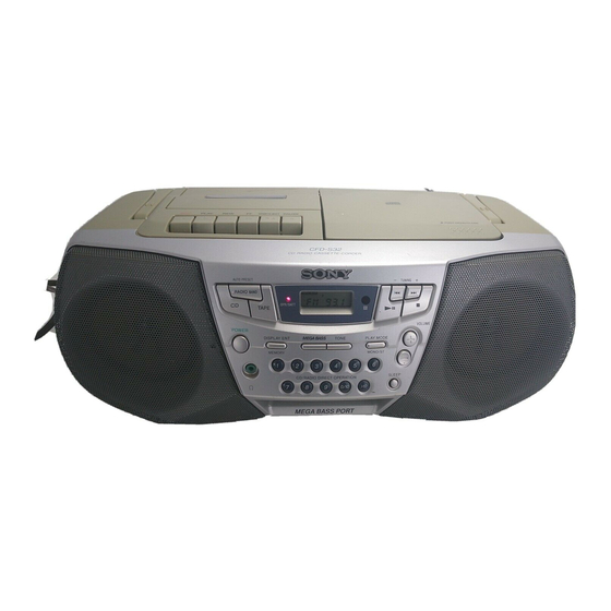
CFD-S22/S32
Photo: CFD-S32 (Silver)
Model Name Using Similar Mechanism CFD-S38
CD
CD Mechanism Type
Section
Optical Pick-up Name
Model Name Using Similar Mechanism CFD-S38
TC
Section Tape Transport Mechanism Type
SPECIFICATIONS
Radio section
Frequency range
US, CND, E92, MX model:
FM: 87.6 - 108 MHz
AM: 530 - 1,710 kHz
SP, AR, AUS, E4, JE model:
FM: 87.5 - 108 MHz or 87.6 - 108 MHz
AM: 531 - 1,602 kHz
Antennas
FM: Telescopic antennas
AM: Built-in ferrite bar antennas
Cassette-corder section
Recording system
4-track 2 channel stereo
Fast winding time
Approx. 120 sec. with Sony cassette C-60
Frequency response
TYPE I (normal): 70 - 10,000 Hz
General
Speaker
Full range: 10 cm (4 in.) dia.,
3.2 ohms, cone type (2)
Outputs
Headphones jack (stereo minijack)
For 16 - 68 ohms impedance headphones
CD RADIO CASSETTE-CORDER
– 1 –
US Model
Canadian Model
E Model
Australian Model
CFD-S22/S32
Tourist Model
CFD-S22
KSM-213CDM
KSS-213C
MF-S22-117
– Continued on next page –
Advertisement
Chapters
Table of Contents

Related Manuals for Sony CFD-S22


Summary of Contents for Sony CFD-S22
- Page 1 Laser diode properties 4-track 2 channel stereo Material: GaAlAs Fast winding time Wave length: 780 nm Approx. 120 sec. with Sony cassette C-60 Emission duration: Continuous Frequency response Laser output: Less than 44.6 µW TYPE I (normal): 70 - 10,000 Hz...
- Page 2 LES COMPOSANTS IDENTIFIÉS PAR UNE MARQUE 0 SUR LES DIAGRAMMES SCHÉMATIQUES ET LA LISTE DES PIÈCES SONT CRITIQUES POUR LA SÉCURITÉ DE FONCTIONNEMENT. NE REMPLACER CES COMPOSANTS QUE PAR DES PIÈCES SONY DONT LES NUMÉROS SONT DONNÉS DANS CE MANUEL OU DANS LES SUPPLÉMENTS PUBLIÉS PAR SONY.
-
Page 3: Table Of Contents
SAFETY CHECK-OUT TABLE OF CONTENTS 1. SERVICING NOTES After correcting the original service problem, perform the following ............4 safety check before releasing the set to the customer: Check the antenna terminals, metal trim, “metallized” knobs, screws, 2. GENERAL and all other exposed metal parts for AC leakage. Check leakage as Location of controls .............. -
Page 4: Servicing Notes
SECTION 1 SERVICING NOTES LASER DIODE AND FOCUS SEARCH OPERATION CHUCK PLATE JIG ON REPAIRING CHECK 1. Turn ON the POWER button and press FUNCTION button to On repairing CD section, playing a disc without the lid (CD), use CD position. Chuck Plate Jig. -
Page 5: General
SECTION 2 GENERAL This section is extracted from instruction manual. Location of controls Remote Control (CFD-S32only) TONE (CFD-S32only) SLEEP CD compartment TAPE Tape compartment RADIO BAND AUTO PRESET OPR/BATT PLAY MODE indicator Z PUSH OPEN/CLOSE MONO/ST POWER FUNCTION Number buttons MODE* BAND VOL +,–... -
Page 6: Playing A Cd
Playing a CD Listening to the radio Press CD (direct power-on). Press RADIO BAND•AUTO PRESET until the band you want appears in the display (direct power-on). Each time you press the button, the indication changes as follows: “FM1” t “FM2” t “AM”. Display Press Z PUSH OPEN/CLOSE down to open the CD compartment and place a CD in the CD compartment. -
Page 7: Playing A Tape
Use TYPE I (normal) tape only. Use TYPE I (normal) tape only. Playing a tape Recording Press xZ to open the tape compartment and insert a Press TAPE (direct power-on). blank tape. With the side you want to Display record on facing upward Press xZ to open the tape compartment and insert a recorded tape. -
Page 8: Disassembly
SECTION 3 DISASSEMBLY • The equipment can be removed using the following procedure. Cabinet (Upper) Assy Cabinet (Front) Sub Assy Wires Main Board Secondary, Power Board Tuner Board VOL SEL Board Tape Mechanism Block Holder Assy, Cassette CD Mechanism Block PRE Board Note : Follow the disassembly procedure in the numerical order given. -
Page 9: Wires
3-2. WIRES Put flat cable and wires between the cabinets and push them in the grooves located at A to G in the figure to prevent disconnection before assembling the set. CABINET (FRONT) CABINET (REAR) from SP 3-3. SECONDARY BOARD, POWER BOARD 6 CN905 5 CNP901 3 BVTP 3x10... -
Page 10: Vol Sel Board
3-4. VOL SEL BOARD (E4 model only) • Abbreviation : AC 110-120V/220-240V area in E model 2 cover (VOL SEL) 3 VOL SEL board 1 BVTP 3x10 3-5. TUNER BOARD 5 TUNER board 1 CNP1 3 holder (PWB)(TU) 2 BVTP 3x10 –... -
Page 11: Cabinet (Upper) Assy
3-6. CABINET (UPPER) ASSY 6 BVTP 3x12 3 holder assy, cassette 7 BVTP 3x12 4 lid (CD) 5 BVTP 3x10 8 BVTP 3x12 9 handle 0 cabinet (upper) assy cabinet (rear) 2 CNP902 1 CNP1 3-7. MAIN BOARD 2 BVTP 3x10 1 BVTP 3x10 8 MAIN board 5 CNP322... -
Page 12: Cd Mechanism Block
3-8. CD MECHANISM BLOCK 1 PWH 2.6x10 2 PWH 2.6x10 3 CD mechanism block (KSM-213CDM) 3-9. TAPE MECHANISM BLOCK 1 BVTP 3x10 2 BVTP 3x10 3 tape mechanism block (MF-S22-117) – 12 –... -
Page 13: Holder Assy, Cassette
3-10. HOLDER ASSY, CASSETTE 1 BVTP 3x10 2 DAMPER 4 holder assy, cassette 3-11. PRE BOARD 1 BVTP 2x4 2 PRE board 3 Removal the solders. – 13 –... -
Page 14: Mechanical Adjustments
SECTION 5 SECTION 4 MECHANICAL ADJUSTMENTS ELECTRICAL ADJUSTMENTS PRECAUTION TAPE SECTION 0 dB = 0.775 V 1. Clean the following parts with a denatured-alcohol-moistened swab : • Standard Output Level record/playback head pinch roller Output terminal HP OUT erase head rubber belts load impedance capstan... -
Page 15: Tuner Section
TUNER SECTION 0 dB = 1 µV FM FREQUENCY COVERAGE • FM Section ADJUSTMENT Setting: Frequency Display 87.5 MHz 108 MHz RADIO (BAND) button: FM Reading on Digital voltmeter 1.6 ± 0.4 V 4.0 ± 0.3V Adjustment Part <confirmation> FM RF signal generator TP (JW2) FM TRACKING ADJUSTMENT... -
Page 16: Cd Section
Adjustment Location: ANT1 TELESCOPIC ANTENNA – tuner board (conductor side) – – tuner board (component side) – TRACKING ADJUSTMENT FREQUENCY COVERAGE ADJUSTMENT TP(VT) (VT) (VT) TRACKING ADJUSTMENT CNP1 CD SECTION CD section adjustments are done automatically in this set. In case of operation check, confirm that focus bias. FOCUS BIAS CHECK Test Point: 1. -
Page 17: Diagrams
SECTION 6 DIAGRAMS 6-1. IC PIN DESCRIPTION Pin No. Pin Name Pin Description • IC501 CXP83620-022Q (SYSTEM CONTROL) — Not used. (Open) Pin No. Pin Name Pin Description A-MUTE Audio mute output H: Mute C-SCOR CD SCOR input EEPROM clock output Sircs receiver input Event counter input MUTE... -
Page 18: Block Diagram - Cd Section
CFD-S22/S32 6-3. BLOCK DIAGRAM — CD SECTION — CD BOARD MAIN BOARD (1/2) SYSTEM SERVO PROCESSOR, DIGITAL SIGNAL PROCESSOR RF AMP IC702 CNP702(2/2) CNP502(2/2) CNP505(1/3) ASYMMETRY IC701 CNP701 CD L CORRECTION AOUT1 RFAC OVER & EFM DEMODULATOR SAMPLING DIGITAL LOUT1... -
Page 19: Block Diagram - Main Section
CFD-S22/S32 6-4. BLOCK DIAGRAM — MAIN SECTION — PRE BOARD MAIN BOARD (2/2) R.RO R.IN R.LIN CD R VOLUME/SOUND CONTROL REC/PB POWER AMP CNP301 CNP505 IC302 PRE AMP IC304 R-CH (3/3) (3/3) CNP301(1/3) IC301 L.RO J321 ALC 2 LINE CD L L.LIN... -
Page 20: Printed Wiring Board - Tuner Section
CFD-S22/S32 6-5. PRINTED WIRING BOARD — TUNER SECTION — • Refer to page 18 for Circuit Boards Location. • Semiconductor Location Ref. No. Location US, CND, E92, MX MODEL E4, SP, AR, AUS, JE MODEL JC25 TP(VT) Note on Printed Wiring Boards: •... -
Page 21: Schematic Diagram - Tuner Section
CFD-S22/S32 6-6. SCHEMATIC DIAGRAM — TUNER SECTION — • Refer to page 47 for IC Block Diagrams. (Page 36) (Page 36) Note on Schematic Diagram: • All capacitors are in µF unless otherwise noted. pF: µµF • Voltages are taken with a VOM (Input impedance 10 MΩ). -
Page 22: Printed Wiring Board - Cd Section
CFD-S22/S32 6-7. PRINTED WIRING BOARD — CD SECTION — • Refer to page 18 for Circuit Boards Location. • Waveforms (MODE: PLAY) 100mV/div 20nsec/div 2.2Vp-p • Semiconductor Location 16.9344MHz IC702 (XTAO) Ref. No. Location IC701 100mV/div 2 sec/div IC702 IC703... - Page 23 CFD-S22/S32 6-8. SCHEMATIC DIAGRAM — CD SECTION — • Refer to page 47 for IC Block Diagrams. (Page 35) Note on Schematic Diagram: • All capacitors are in µF unless otherwise noted. pF: µµF • Power voltage is dc 9V and fed with regulated dc power 50 WV or less are not indicated except for electrolytics supply from battery terminal.
- Page 24 CFD-S22/S32 6-9. SCHEMATIC DIAGRAM — PRE SECTION — • Refer to page 48 for IC Block Diagrams. • Semiconductor Location Ref. No. Location Ref. No. Location D322 G-11 Q124 G-12 D323 H-11 Q221 E-11 D324 B-10 Q222 E-11 (D506) (Q223)
-
Page 25: Printed Wiring Boards - Main Section
CFD-S22/S32 6-10. PRINTED WIRING BOARDS — MAIN SECTION — • Refer to page 18 for Circuit Boards Location. (Page 23) (Page 28) (Page 43) L-CH R-CH (Page 23) LIQUID CRYSTAL DISPLAY PANEL EXCEPT E4,SP,AR,AUS,JE MODEL E4,SP,AR,AUS,JE MODEL (Page 40) – 33 –... -
Page 26: Schematic Diagram - Main Section (1/2)
CFD-S22/S32 6-11. SCHEMATIC DIAGRAM — MAIN SECTION (1/2) — • Refer to page 32 for Note on Schematic Diagram and page 48 for IC Block Diagrams. R594 680 : E4,SP,AR,JE MODEL (Page 32) 1.5k : AUS MODEL JW : EXCEPT E4,SP,AR AUS,JE MODEL... -
Page 27: Schematic Diagram - Main Section (2/2)
CFD-S22/S32 6-12. SCHEMATIC DIAGRAM — MAIN SECTION (2/2) — • Refer to page 32 for Note on Schematic Diagram and page 48 for IC Block Diagrams. KTC3198GR-AT KTC3198GR-AT KTC3198GR-AT KTC3198GR-AT (Page 35) (Page 46) – 37 – – 38 –... -
Page 28: Printed Wiring Board - Control Section
CFD-S22/S32 6-13. PRINTED WIRING BOARD — CONTROL SECTION — • Refer to page 18 for Circuit Boards Location. (Page 33) OPR/BATT • Semiconductor Location Ref. No. Location D601 Note on Printed Wiring Boards: (IC601) G-10 • X : parts extracted from the component side. - Page 29 CFD-S22/S32 6-14. SCHEMATIC DIAGRAM — CONTORL SECTION — (Page 36) Note on Schematic Diagram: • All capacitors are in µF unless otherwise noted. pF: µµF 50 WV or less are not indicated except for electrolytics and tantalums. • All resistors are in W or less unless otherwise specified.
-
Page 30: Printed Wiring Boards - Power Supply Section
CFD-S22/S32 6-15. PRINTED WIRING BOARDS — POWER SUPPLY SECTION — • Refer to page 18 for Circuit Boards Location. • Semiconductor Location Ref. No. Location D901 J-10 D902 I-10 DRY BATTERY SIZE " D " D903 (IEC DESIGNATION R20) D904 3PCS, 4.5V... -
Page 31: Schematic Diagram - Power Supply Section
CFD-S22/S32 6-16. SCHEMATIC DIAGRAM — POWER SUPPLY SECTION — (Page 38) Note on Schematic Diagram: • All capacitors are in µF unless otherwise noted. pF: µµF 50 WV or less are not indicated except for electrolytics and tantalums. • C : panel designation. - Page 32 • IC Block Diagrams IC1 TA2149N IC701 CXA2550M IC301 TA2068N GND1 LINE FM RF FM RF-OUT L.LIN L.PO AGCVTH VCC1 FM RF-IN MIC I/EX AMP1 AM RF-IN BUF AMP TAPE APC PD APC LD L.NF RADIO AM LOW CUT L.RAD LD ON MIX OUT FM OSC...
- Page 33 IC702 CXD2587Q ERROR DIGITAL ASYMMETRY DIGITAL CORRECTOR CORRECTION LRCK OPERATIONAL AMPLIFIER PCMD INTERFACE DEMODULATOR ANALOG SWITCH CONVERTER EMPH XVDD CLOCK XTSL GENERATOR XTAI TIMING TES1 XTAO LOGIC TEST XVSS SERVO DSP PWM GENERATOR AVDD1 FRDR FOCUS FOCUS PWM AOUT1 SERVO GENERATOR FFDR AIN1...
-
Page 34: Exploded Views
SECTION 7 EXPLODED VIEWS NOTE: • The mechanical parts with no reference • Color Indication of Appearance Parts The components identified by mark 0 or dotted line with mark number in the exploded views are not supplied. Example : 0 are critical for safety. •... -
Page 35: Cabinet (Rear) Section
7-2. CABINET (REAR) SECTION F901 T901 F902 S901 The components identified by Les composants identifiés par une mark 0 or dotted line with mark marque 0 sont critiques pour la 0 are critical for safety. sécurité. Replace only with part number Ne les remplacer que par une piéce specified. -
Page 36: Cabinet (Upper) Section
7-3. CABINET (UPPER) SECTION ANT1 S501 LCD501 MF-S22-117 not supplied KSM-213CDM – 52 –... - Page 37 Ref. No. Part No. Description Remark Ref. No. Part No. Description Remark * 101 A-3322-449-A MAIN BOARD, COMPLETE (S22:US) 1-792-205-11 CABLE, FLEXIBLE FLAT (21 CORE) * 101 A-3322-471-A MAIN BOARD, COMPLETE (S32:US) * 112 3-041-646-01 HOLDER (LCD) * 101 A-3322-557-A MAIN BOARD, COMPLETE (S22:SP,AR) * 113 1-676-531-11 LCD BOARD * 101...
-
Page 38: Tape Mechanism Section-1
7-4. TAPE MECHANISM SECTION-1 (MF-S22-117) HRP301 HE301 Ref. No. Part No. Description Remark Ref. No. Part No. Description Remark 3-933-010-01 SPRING (S/P), TORSION * 162 3-008-587-01 SLIDER (STOP) 3-933-025-01 SPRING (P), TORSION * 163 3-008-591-01 SLIDER (PAUSE) 3-040-857-01 LEVER (P) 3-933-004-01 CLAW, REEL 3-933-024-01 ROLLER, PINCH * 165... -
Page 39: Tape Mechanism Section-2
7-5. TAPE MECHANISM SECTION-2 (MF-S22-117) S304 M301 Ref. No. Part No. Description Remark Ref. No. Part No. Description Remark 3-933-029-01 LEVER, ERASING PREVENTION X-3372-924-1 FLYWHEEL ASSY 3-933-182-01 SPRING, CASSETTE 3-932-993-01 CHASSIS, OUTSERT 3-932-995-01 GEAR (MID) 3-343-358-01 RING, RETAINING X-3371-667-1 CLUTCH ASSY 3-933-005-01 SPRING (CAM), COMPRESSION 3-932-997-01 GEAR (CAM) 3-016-349-01 WASHER... -
Page 40: Optical Pick-Up Section
7-6. OPTICAL PICK-UP SECTION (KSM-213CDM) not supplied M701 M702 The components identified by Les composants identifiés par une mark 0 or dotted line with mark marque 0 sont critiques pour la 0 are critical for safety. sécurité. Replace only with part number Ne les remplacer que par une piéce specified. -
Page 41: Electrical Parts List
SECTION 8 BATTERY ELECTRICAL PARTS LIST NOTE: • Due to standardization, replacements in • RESISTORS The components identified by mark 0 or dotted line with mark the parts list may be different from the All resistors are in ohms. 0 are critical for safety. parts specified in the diagrams or the METAL:Metal-film resistor. - Page 42 Ref. No. Part No. Description Remark Ref. No. Part No. Description Remark JC715 1-216-295-00 SHORT JC770 1-216-295-00 SHORT JC716 1-216-295-00 SHORT JC771 1-216-295-00 SHORT JC717 1-216-295-00 SHORT JC772 1-216-295-00 SHORT JC718 1-216-295-00 SHORT JC773 1-216-295-00 SHORT JC719 1-216-295-00 SHORT JC774 1-216-295-00 SHORT JC720 1-216-295-00 SHORT...
- Page 43 Ver. 1.4 CONTROL Ref. No. Part No. Description Remark Ref. No. Part No. Description Remark R759 1-216-097-11 RES-CHIP 100K 1/10W R604 1-249-420-11 CARBON 1.8K 1/4W R760 1-216-246-00 RES-CHIP 100K 1/8W R605 1-249-429-11 CARBON 1/4W R761 1-216-097-11 RES-CHIP 100K 1/10W R606 1-249-432-11 CARBON 1/4W R762...
- Page 44 CONTROL HALF BATTERY MAIN Ref. No. Part No. Description Remark Ref. No. Part No. Description Remark S626 1-762-798-11 SWITCH, KEY BOARD (8) C130 1-104-665-11 ELECT 100uF S627 1-762-798-11 SWITCH, KEY BOARD (TONE) (S32) C131 1-126-926-11 ELECT 1000uF C132 1-136-165-00 MYLAR 0.1uF ************************************************************* C221...
- Page 45 MAIN Ref. No. Part No. Description Remark Ref. No. Part No. Description Remark C541 1-126-960-11 ELECT * KH503 1-565-386-11 HOLDER, CABLE 5P C542 1-162-306-11 CERAMIC 0.01uF C543 1-162-282-31 CERAMIC 100PF < TRANSISTOR > C544 1-162-282-31 CERAMIC 100PF C545 1-162-294-31 CERAMIC 0.001uF Q121 8-729-036-89 TRANSISTOR KTC3198GR-AT...
- Page 46 MAIN Ref. No. Part No. Description Remark Ref. No. Part No. Description Remark R226 1-249-421-11 CARBON 2.2K 1/4W R562 1-249-425-11 CARBON 4.7K 1/4W (US,CND,AUS) R563 1-249-429-11 CARBON 1/4W R227 1-249-429-11 CARBON 1/4W (S32) R228 1-249-415-11 CARBON 1/4W R565 1-249-417-11 CARBON 1/4W R230 1-247-815-11 CARBON...
- Page 47 POWER SECONDARY Ref. No. Part No. Description Remark Ref. No. Part No. Description Remark 1-676-530-11 POWER BOARD < RESISTOR > ************* R101 1-216-077-11 RES-CHIP 1/10W 1-533-233-31 HOLDER, FUSE (E4) R102 1-216-023-00 METAL CHIP 1/10W R103 1-216-097-11 RES-CHIP 100K 1/10W < CAPACITOR > R104 1-216-061-00 METAL CHIP 3.3K...
- Page 48 TUNER Ref. No. Part No. Description Remark Ref. No. Part No. Description Remark A-3322-456-A TUNER BOARD, COMPLETE (US,CND,E92,MX) 1-163-251-11 CERAMIC CHIP 100PF A-3322-558-A TUNER BOARD, COMPLETE (SP,AR) 1-163-251-11 CERAMIC CHIP 100PF A-3322-621-A TUNER BOARD, COMPLETE (AUS) 1-163-251-11 CERAMIC CHIP 100PF A-3322-694-A TUNER BOARD, COMPLETE (E4,JE) 1-163-251-11 CERAMIC CHIP 100PF...
- Page 49 TUNER Ref. No. Part No. Description Remark Ref. No. Part No. Description Remark JC30 1-216-295-00 SHORT 1-419-465-11 COIL (DET) JC31 1-216-295-00 SHORT JC33 1-216-295-00 SHORT < VIBRATOR > JC38 1-216-295-00 SHORT JC39 1-216-295-00 SHORT 1-760-130-11 VIBRATOR, CRYSTAL (75kHz) (E4,SP,AR,JE) 1-781-592-11 VIBRATOR, CRYSTAL (75kHz) JC40 1-216-295-00 SHORT (US,CND,E92,MX,AUS)
- Page 50 CFD-S22/S32 Ver. 1.5 Ref. No. Part No. Description Remark ACCESSORIES ************ 1-557-287-11 CORD, POWER (E92,MX) 1-569-008-21 ADAPTOR, CONVERSION (2P) (E4,JE) 1-690-952-11 CORD, POWER (CND) 1-696-819-11 CORD, POWER (AUS) 1-769-412-11 CORD, POWER (E4,SP,JE) 1-782-126-11 CORD, POWER (US) 1-783-952-11 CORD, POWER (AR)
- Page 51 CFD-S22/S32 US Model Canadian Model SERVICE MANUAL E Model Australian Model CFD-S22/S32 Ver 1.3 2001.03 Tourist Model CFD-S22 SUPPLEMENT-1 File this supplement with the service manual. Subject : 1. Change of CD Board 2. Change of Main Board (ECN-RCA01778) IC pin description, block diagram, printed wiring board, schematic diagram of new type, and changed parts list are described in this Supplement-1.
- Page 52 TABLE OF CONTENTS – MAIN BOARD (COMPONENT SIDE) – 1. Exploded Views ..............3 2. Electrical Adjustment ............4 3. IC Pin Description ..............5 4. Block Diagram –CD Section– ..........7 5. Printed Wiring Board –CD Section– ........9 6.
-
Page 53: Exploded Views
1. EXPLODED VIEWS : indicates changed portion. Page FORMER TYPE NEW TYPE MF-S22-117 not supplied KSM-213CDM Ref. No. Part No. Description Remark Part No. Description Remark * 101 A-3322-449-A MAIN BOARD, COMPLETE (S22:US) A-3322-670-A MAIN BOARD, COMPLETE (S22:US) * 101 A-3322-471-A MAIN BOARD, COMPLETE (S32:US) A-3322-667-A MAIN BOARD, COMPLETE (S32:US) * 101... -
Page 54: Electrical Adjustment
2. ELECTRICAL ADJUSTMENT CD SECTION CD section adjustments are done automatically in this set. In case of operation check, confirm that focus bias. FOCUS BIAS CHECK Test Point: 1. Connect the oscilloscope between IC701 pin wj (or TP (RF)) – CD board (conductor side) – and GND on CD board. -
Page 55: Ic Pin Description
3. IC PIN DESCRIPTION • IC501 CXP83620-025Q/026Q (SYSTEM CONTROL) Pin No. Pin Name Pin Description CD WRQ signal input Sircs receiver input MUTE MUTE output H: Mute F TEX frequency division output FSEQ CD SENSE read clock input C-CE CD chip enable output C-CL CD clock output C-DI... - Page 56 Pin No. Pin Name Pin Description — Not used. (Open) A-MUTE Audio mute output H: Mute EEPROM clock output Event counter input TC-PLAY Tape play switch input L: Tape C-DOOR CD door open/close switch input L: Close – 6 –...
-
Page 57: Block Diagram -Cd Section
CFD-S22/S32 4. BLOCK DIAGRAM — CD SECTION — CD BOARD MAIN BOARD (1/2) CNP702(2/2) CN502(2/2) CNP505(1/3) RF AMP AGON LCHO CD L IC701 INTERPOLATION CNP701 ERROR SLICE MUTE DIGITAL FIN2 EFMIN CORRECTION LEVEL & FILTER AUDIO CD CONTROL CONTROL RCHO ATTENUATION &... -
Page 58: Printed Wiring Board -Cd Section
CFD-S22/S32 5. PRINTED WIRING BOARD — CD SECTION — • Waveforms (MODE: PLAY) 100mV/div 20 sec/div 1.8V • Semiconductor Location Approx. 100mVp-p IC701 (TE) Ref. No. Location D701 100mV/div 20 sec/div IC701 IC702 1.8V IC703 Approx. 100mVp-p Q701 IC701 (FE) 500mV/div 0.5 sec/div... -
Page 59: Schematic Diagram -Cd Section
CFD-S22/S32 6. SCHEMATIC DIAGRAM — CD SECTION — • Refer to page 19 for IC Block Diagrams. ((Page 15)) Note on Schematic Diagram: • U : B+ Line. • All capacitors are in µF unless otherwise noted. pF: µµF • Circled numbers refer to waveforms. -
Page 60: Printed Wiring Board -Main Section
CFD-S22/S32 7. PRINTED WIRING BOARD — MAIN SECTION — • Semiconductor Location Ref. No. Location Ref. No. Location (Page 23) D322 (Q123) D323 Q124 Q221 D324 (D506) Q222 (D507) (Q223) (D508) Q224 D509 Q501 D510 Q502 D511 Q503 [D951] Q504... -
Page 61: Schematic Diagram -Main Section (1/2)
CFD-S22/S32 8. SCHEMATIC DIAGRAM — MAIN SECTION (1/2) — • Refer to page 14 for Note on Schematic Diagram. (Page 32) (Page 41) ((Page 17)) (Page 26) (Page 26) ((Page 12)) – 15 – – 16 –... -
Page 62: Schematic Diagram -Main Section (2/2)
CFD-S22/S32 9. SCHEMATIC DIAGRAM — MAIN SECTION (2/2) — • Refer to page 14 for Note on Schematic Diagram. ((Page 15)) (Page 46) – 17 – – 18 –... -
Page 63: Ic Block Diagrams
10. IC BLOCK DIAGRAMS IC702 LC78641NE IC701 LA9235M ODRV FIN1 78 77 76 75 74 73 72 71 68 67 66 65 RFSW – FIN2 AGCON – – TIN1 AUTO ADJUST PH(RFENV) – TIN2 VREF DVREF/FC JITTV DEEFECT – – SERVO ODRV JITTC... -
Page 64: Electrical Parts List
MAIN 11. ELECTRICAL PARTS LIST NOTE: Ref. No. Part No. Description Remark Ref. No. Part No. Description Remark • RESISTORS • SEMICONDUCTORS • Due to standardization, replacements in R713 1-216-831-11 METAL CHIP 6.8K 1/16W C123 1-126-961-11 ELECT 2.2uF All resistors are in ohms. In each case, u : µ, for example: the parts list may be different from the R714... - Page 65 MAIN Ref. No. Part No. Description Remark Ref. No. Part No. Description Remark C519 1-126-964-11 ELECT 10uF IC304 8-759-426-51 IC BA5417 (S32) % IC501 8-752-918-83 IC CXP83620-026Q C520 1-104-664-11 ELECT 47uF IC502 8-759-658-46 IC S-81233SGY-Z (S32) IC503 8-759-645-87 IC PST9128-T C522 1-104-665-11 ELECT 100uF...
- Page 66 MAIN Ref. No. Part No. Description Remark Ref. No. Part No. Description Remark R126 1-249-417-11 CARBON 1/4W R529 1-249-417-11 CARBON 1/4W (E4,E92,SP,AR,MX,JE) R530 1-249-429-11 CARBON 1/4W R126 1-249-421-11 CARBON 2.2K 1/4W R534 1-247-843-11 CARBON 3.3K 1/4W (US,CND,AUS) R535 1-249-429-11 CARBON 1/4W R127 1-249-429-11 CARBON...
- Page 67 MAIN Ref. No. Part No. Description Remark R958 1-249-411-11 CARBON 1/4W R960 1-249-393-11 CARBON 1/4W R961 1-249-417-11 CARBON 1/4W R997 1-249-429-11 CARBON 1/4W < VIBRATOR > X501 1-781-775-11 VIBRATOR, CERAMIC (4.19MHz) X502 1-781-721-11 VIBRATOR, CRYSTAL (150kHz) – 25 –...
- Page 68 CFD-S22/S32 REVISION HISTORY Clicking the version allows you to jump to the revised page. Also, clicking the version at the upper on the revised page allows you to jump to the next revised page. Ver. Date Description of Revision 1997.10 2000.04...