Table of Contents
Advertisement
Quick Links
SERVICE MANUAL
Ver 1.0 2001.04
HCD-DX90 is the tuner, deck, CD and
amplifier section in MHC-DX90.
Amplifier section
CD player section
Sony Corporation
9-873-882-11
2001D0500-1
Home Audio Company
C 2001.4
Shinagawa Tec Service Manual Production Group
HCD-DX90
Model Name Using Similar Mechanism
CD
CD Mechanism Type
SECTION
Base Unit Type
Optical Pick-up Type
Model Name Using Similar Mechanism
TAPE DECK
SECTION
Tape Transport Mechanism Type
SPECIFICATIONS
Tape player section
Tuner section
FM tuner section
COMPACT DISC DECK RECEIVER
E Model
HCD-BX9/DX9
CDM58-K2BD38
BU-K2BD38
KSM-213DAP
NEW
TCM-230AWP11
AM tuner section
General
Advertisement
Table of Contents

Related Manuals for Sony HCD-DX90


Summary of Contents for Sony HCD-DX90
- Page 1 HCD-DX90 SERVICE MANUAL E Model Ver 1.0 2001.04 HCD-DX90 is the tuner, deck, CD and amplifier section in MHC-DX90. Model Name Using Similar Mechanism HCD-BX9/DX9 CD Mechanism Type CDM58-K2BD38 SECTION Base Unit Type BU-K2BD38 Optical Pick-up Type KSM-213DAP Model Name Using Similar Mechanism...
-
Page 2: Table Of Contents
COMPONENTS IDENTIFIED BY MARK 0 OR DOTTED LINE WITH MARK 0 ON THE SCHEMATIC DIAGRAMS AND IN THE PARTS LIST ARE CRITICAL TO SAFE OPERATION. REPLACE THESE COMPONENTS WITH SONY PARTS WHOSE PART NUMBERS APPEAR AS SHOWN IN THIS MANUAL OR IN SUPPLEMENTS PUBLISHED BY SONY. -
Page 3: Service Note
HCD-DX90 SECTION 1 SERVICE NOTE Note for installing the panel board 2 panel board Hot melt 1 Cut the thirteen melted-connection points with a cutting plier. Screw hole Attach the panel board with eleven screws ( +BVTP 2.6 8 ) after the board is removed once. -
Page 4: General
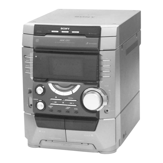
HCD-DX90 SECTION 2 GENERAL LOCATION OF CONTROLS 2 3 4 DISC SKIP EX-CHANGE button V-GROOVE button and indicator DISC 1 button and indicator CURSOR button and indicator DISC 2 button and indicator GROOVE button DISC 3 button and indicator EQ EDIT button... - Page 5 HCD-DX90 This section is extracted from instruction manual. Step 2: Setting the Press ENTER. The minute indication flashes. time You must set the time before using the timer functions. The clock is on a 24-hour system for the European model and a 12-hour system for other models.
-
Page 6: Disassembly
HCD-DX90 SECTION 3 DISASSEMBLY • This set can be disassembled in the order shown below. 3-1. DISASSEMBLY FLOW 3-2. UPPER CASE (TOP) (page 7) 3-3. LOADING PANEL ASSY (page 7) 3-4. FRONT PANEL SECTION, CD MECHANISM DECK (CDM58-K2BD38) (page 8) 3-5. -
Page 7: Upper Case (Top)
HCD-DX90 Note: Follow the disassembly procedure in the numerical order given. 3-2. UPPER CASE (TOP) 9 two screws (+BVTP 3 qs upper case (top) 5 two screws (case 3 TP2) 7 two screws (+BVTP 3 0 claw side panel (R) -
Page 8: Front Panel Section, Cd Mechanism Deck (Cdm58-K2Bd38)
HCD-DX90 3-4. FRONT PANEL SECTION, CD MECHANISM DECK (CDM58-K2BD38) 9 connector (CN201) qs CD mechanism deck (CDM58) 4 screw (+BVTP 3 Connector (CN601) 1 flat type wire (CN304) 5 screw (+BVTP 3 2 connector (CN1) 0 connector (CN202) 3 connector (CN2) -
Page 9: Panel Board
HCD-DX90 3-6. PANEL BOARD 0 three claws 9 two screws (+BVTP 2.6 7 knob(MIC) qa CD Switch board 6 spring 2 two screws qf panel board (+BVTP 2.6 qd five claws 3 two bosses & four pins 5 FR knob qs Cut the thirteen melted-connection points with a cutting plier. -
Page 10: Main Board, Amp Board
HCD-DX90 3-8. MAIN BOARD, AMP BOARD 5 three screws (+BVTP 3 8 heat sink 7 two screws (+BVTP 3 6 POWER AMP board 2 connector(CN502) 4 two screws (+BVTP 3 2 connector (CN503) 3 MAIN board 1 two screws (+BVTP 3 3-9. -
Page 11: Base Unit (Bu-K2Bd38)
HCD-DX90 3-10. BASE UNIT (BU-K2BD38) 8 two insulators base unit (BU-K2BD38) 1 flat type wire (CN101) 9 two insulators 6 two springs (insulator), coil 5 stopper (BU) 3 two springs (insulator), coil 2 two screws (+PTPWH 2.6), floating 4 two screws (+PTPWH 2.6) 3-11. -
Page 12: Test Mode
HCD-DX90 SECTION 4 TEST MODE [MC Cold Reset] [Change-over of MW Tuner Step between 9 kHz and • The cold reset clears all data including preset data stored in the 10 kHz] RAM to initial conditions. Execute this mode when returning •... - Page 13 HCD-DX90 [MC Test Mode] • This mode is used to check operations of the respective sections of Amplifier, Tuner, CD and Tape. Procedure: Press the ?/1 button to turn on the set. Press the three buttons of x , ENTER and DISC 3 simultaneously.
- Page 14 HCD-DX90 [Aging Mode] This mode can be used for operation check of CD section and tape deck section. • If an error occurred: The aging operation stops and display status. • If no error occurs: The aging operation continues repeatedly.
- Page 15 HCD-DX90 2) Operation during aging mode In the aging mode, the program is executed in the following sequence. (1) The disc tray opens and closes. (2) The mechanism accesses DISC 2 and makes an attempt to read TOC. However, since there are no discs, a message “CD2 NO DISC”...
-
Page 16: Mechanical Adjustments
HCD-DX90 SECTION 5 SECTION 6 MECHANICAL ADJUSTMENTS ELECTRICAL ADJUSTMENTS Precaution DECK SECTION 0 dB=0.775 V 1. Clean the following parts with a denatured alcohol-moistened swab: 1. Demagnetize the record/playback head with a head record/playback heads pinch rollers demagnetizer. erase head rubber belts 2. - Page 17 HCD-DX90 2. Turn the adjustment screw and check output peaks. If the peaks DECK B Tape Speed Adjustment do not match for L-CH and R-CH, turn the adjustment screw Note: Start the Tape Speed adjustment as below after setting to the test so that outputs match within 1dB of peak.
- Page 18 HCD-DX90 DECK B REC Bias Adjustment 4. Mode: Record Procedure: INTRODUCTION MD/VIDEO (AUDIO) IN When set to the test mode performed in Tape Speed Adjustment, 315 Hz, 50 mV (–23.8 dB) AF OSC when the tape is rewound after recording, the “REC memory mode”...
- Page 19 HCD-DX90 FM Tuned Level Adjustment CD SECTION FM RF SSG Note : 1. CD Block is basically designed to operate without adjustment. coaxial Therefore, check each item in order given. 2. Use YEDS-18 disc (3-702-101-01) unless otherwise indicated. 3. Use an oscilloscope with more than 10M impedance.
- Page 20 HCD-DX90 Note: Clear RF signal waveform means that the shape “ ” can be Adjustment Location: clearly distinguished at the center of the waveform. [BD BOARD] (Conductor Side) RF signal waveform VOLT/DIV : 200mV TIME/DIV : 500ns level : 1.45 0.3Vp-p...
-
Page 21: Diagrams
HCD-DX90 SECTION 7 DIAGRAMS 7-1. CIRCUIT BOARDS LOCATION THIS NOTE IS COMMON FOR PRINTED WIRING BOARDS AND SCHEMATIC DIAGRAMS. (In addition to this, the necessary note is printed in each block.) MOTOR Board DRIVER Board Note on Schematic Diagram: Note on Printed Wiring Boards: •... -
Page 22: Block Diagrams
HCD-DX90 AM/FM IF MPX 7-2. BLOCK DIAGRAMS TM601 LPF601 Q602 IC601 CF601 CF602 – TUNER/CD SECTION – RF IF BUFFER L-CH • RCH is omitted ANT IN IF OUT FM IF L OUT Q611 • Signal Path FM 75 OSC OUT... - Page 23 HCD-DX90 – MAIN SECTION – INPUT SELECT TONE/VOL CONT IC101 IC102 IC501 TM801 (Page 22) L-CH IN2A VOL OUT2 POWER SPEAKER Q504,505 Q861 Q821,822 Q824,825 RY801 LOUT MUTE MUTE MUTE MUTE PROTECT R CH (Page 22) IN2C RELAY CONT Q103...
-
Page 24: Printed Wiring Board - Bd Section
HCD-DX90 7-3. PRINTED WIRING BOARD – BD SECTION – • See page 21 for Circuit Boards Location. • Semiconductor Location Ref. No. Location IC101 IC102 IC103 Q101 TP (TEO) (VC) TP (FEO) (KSM-213DAP) TP (RF) TP (FEI) TP (AGCCON) (GND) -
Page 25: Schematic Diagram - Bd Section
HCD-DX90 7-4. SCHEMATIC DIAGRAM – BD SECTION – • See page 21 for Wavefoms. • See page 42 for IC Block Diagrams. (TEO) (FEO) (VC) (RFO) OPTICAL PICK-UP BLOCK (KSM-213DAP) (AGCCON) (FE1) (XPCK) MAIN BOARD (3/3) CN201 (Page 29) • Voltages and waveforms are dc with respect to ground The components identified by mark 0 or dotted under no-signal conditions. -
Page 26: Printed Wiring Board - Main Section
HCD-DX90 7-5. PRINTED WIRING BOARD – MAIN SECTION – • See page 21 for Circuit Boards Location. • Semiconductor Location Ref. No. Location Ref. No. Location MAIN BOARD IC951 D501 (Page 36) (Page 24) D502 IC961 DRIVER BOARD BD BOARD... -
Page 27: Schematic Diagram - Main (1/3) Section
HCD-DX90 7-6. SCHEMATIC DIAGRAM – MAIN (1/3) SECTION – • See page 43 for IC Block Diagrams. 220p T601 RV611 NULL FM TUNED LEVEL • Voltages and waveforms are dc with respect to ground under no-signal (detuned) conditions. no mark : FM... -
Page 28: Schematic Diagram - Main (2/3) Section
HCD-DX90 7-7. SCHEMATIC DIAGRAM – MAIN (2/3) SECTION – • See page 21 for Wavefoms. • See page 44 for IC Block Diagrams. • See page 34 for Printed Wiring Board of Head Boards. (Page 29) (Page 29) (Page 29) -
Page 29: Schematic Diagram - Main (3/3) Section
HCD-DX90 7-8. SCHEMATIC DIAGRAM – MAIN (3/3) SECTION – (Page 27) (Page 31) (Page 31) MAIN BOARD (1/3) POWER AMP BOARD POWER AMP BOARD M961 CN503 CN502 Q891, 892 FAN DRIVE 3.3k 4.7k C824 BD BOARD CN101 R901 (Page 25) -
Page 30: Printed Wiring Board - Power Amp Section
HCD-DX90 7-9. PRINTED WIRING BOARD – POWER AMP SECTION – • See page 21 for Circuit Boards Location. • Semiconductor Location Ref. No. Location (Page 38) (Page 26) (Page 26) D501 TRANS BOARD MAIN BOARD MAIN BOARD CN977 CN902 CN901... -
Page 31: Schematic Diagram - Power Amp Section
HCD-DX90 7-10. SCHEMATIC DIAGRAM – POWER AMP SECTION – RBV-602 1.5k MTZJ-T-77-15B 0.22 NO505 TRANS BOARD STK-412-040 CN978 0.22 (Page 39) 0.001 TRANS BOARD CN977 (Page 39) TRANS BOARD CN977 (Page 39) 0.001 2SB1375 1.5k MTZJ-T-77-15B 0.22 STK-412-040 0.22 R531... -
Page 32: Printed Wiring Board - Panel Section
HCD-DX90 7-11. PRINTED WIRING BOARD – PANEL SECTION – • See page 21 for Circuit Boards Location. • Semiconductor Location Ref. No. Location CD SW BOARD D601 C-10 D602 D603 D611 D612 D613 D632, S645 D631, S644 D630, S643 D614... -
Page 33: Schematic Diagram - Panel Section
HCD-DX90 7-12. SCHEMATIC DIAGRAM – PANEL SECTION – • See page 21 for Wavefoms. • See page 43 for IC Block Diagrams. 33 50V : /1 MAIN BOARD (3/3) CN401 (Page 29) MTZJ-T-77-5.6C LEVEL REPEAT REC PAUSE/START EDIT DOLBY NR... -
Page 34: Printed Wiring Board - Leaf Sw Section
HCD-DX90 7-13. PRINTED WIRING BOARD – LEAF SW SECTION – • See page 21 for Circuit Boards Location. • See page 28 for Schematic Diagram of Head Board. • Semiconductor Location Ref. No. Location D1001 PM1001 TAPE MECHANISM PM1002 D1002... -
Page 35: Schematic Diagram - Leaf Sw Section
HCD-DX90 7-14. SCHEMATIC DIAGRAM – LEAF SW SECTION – TAPE SPEED (NORMAL) TAPE MECHANISM DECK BLOCK (1/3) TAPE SPEED (HIGH) (TCM-230PWR11) PM1002 PM1001 (DECK-B) (DECK-A) (DECK-A) (DECK-B) MAIN BOARD (2/3) CN304 (Page 28) • Voltages and waveforms are dc with respect to ground under no-signal conditions. -
Page 36: Printed Wiring Board - Driver Section
HCD-DX90 7-15. PRINTED WIRING BOARD – DRIVER SECTION – • Semiconductor Location Ref. No. Location D701 IC701 IC711 (14) (14) (14) CN202 (Page 26) -
Page 37: Schematic Diagram - Driver Section
HCD-DX90 7-16. SCHEMATIC DIAGRAM – DRIVER SECTION – OPEN CLOSE C712 TABLE ADDRESS SENS MAIN BOARD (3/3) CN202 (Page 29) (UP/DOWN) • Voltages and waveforms are dc with respect to ground under no-signal conditions. no mark : CD (STOP) -
Page 38: Printed Wiring Board - Trans Section
HCD-DX90 7-17. PRINTED WIRING BOARD – TRANS SECTION – • See page 21 for Circuit Boards Location. F973 F972 S951 NO506 (Page 30) NO501 CN978 (Page 30) NO504 (Page 30) -
Page 39: Schematic Diagram - Trans Section
HCD-DX90 7-18. SCHEMATIC DIAGRAM – TRANS SECTION – S951 CN978 F973 T4A 250V NO504 (Page 31) F972 T4A 250V CN977 NO501 (Page 31) NO506 (Page 31) The components identified by mark 0 or dotted line with mark 0 are critical for safety. -
Page 40: Ic Pin Function Description
HCD-DX90 7-19. IC PIN FUNCTION DESCRIPTION • MAIN BOARD IC401 M30622MAA-A25FP (MASTER CONTROL) Pin No. Pin Name Description Pin No. Pin Name Description SURROUND 1 Not used. Not used. SURROUND 2 Not used. Not used. SURROUND 3 Not used. Not used. - Page 41 HCD-DX90 • PANEL BOARD IC601 TMP88CP77F-1A22 (DISPLAY CONTROL) Pin No. Pin Name Description VOLUME A VOLUME A signal input. VOLUME B VOLUME B signal input. HEADPHONE Head phone detect signal input. H=ON, L=OFF Not used. TUNER TUNER LED driver output.(high active) CD LED driver output.(high active)
-
Page 42: Ic Block Diagrams
HCD-DX90 7-20. IC BLOCK DIAGRAMS IC101 CXD2587Q (BD BOARD) ERROR ASYMMETRY DIGITAL DIGITAL CORRECTOR CORRECTION LRCK OPERATIONAL AMPLIFIER PCMD INTERFACE DEMODULATOR ANALOG SWITCH CONVERTER EMPH XVDD CLOCK XTSL GENERATOR XTAI TIMING TES1 LOGIC XTAO TEST XVSS SERVO DSP PWM GENERATOR... - Page 43 HCD-DX90 IC103 CXA2568M (BD BOARD) IC602 BA3830F (PANEL BOARD) APC PD AMP REFFERENCE 18 RESET RESET LC/PD CURRENT LD_ON HOLD REFFERENCE 17 f01 CURRENT AGCVTH VREF APC LD AMP HOLD_SW LINE 16 f02 AGCCONT (50%/30% OFF) LINE RF_BOT 15 f03...
- Page 44 HCD-DX90 IC601 BA1450 (MAIN BOARD) AM IF VREG DECODER DRIVER COMP IC302 PC1330H (MAIN BOARD) INVERTER COMPARATER SW R1 SW P1 CONT SW P2 SW R2 IC651 LC72130 (MAIN BOARD) SWALLOW COUNTER 1/16.1/17 4bits POWER REFERENCE RESET DIVIDER SWALLOW COUNTER 1/16.1/17 4bits...
-
Page 45: Exploded Views
HCD-DX90 SECTION 8 EXPLODED VIEWS NOTE: • -XX, -X mean standardized parts, so they may • Abbreviation The components identified by mark 0 or have some differences from the original one. : 120 V AC Area in E model dotted line with mark 0 are critical for safety. -
Page 46: Panel Section
4-224-559-01 CAM(R), HEART 4-225-032-01 VOL KNOB 4-224-561-01 BRACKET (HEART CAM R) 4-225-053-01 SPRING R A-4428-077-A CD SWITCH BOARD, COMPLETE 4-962-708-71 EMBLEM (4-A), SONY A-4476-248-A PANEL BOARD, COMPLETE 4-951-620-01 SCREW (2.6X8), +BVTP 4-225-033-01 FR KNOB X-4953-730-1 FRONT PANEL ASSY 4-224-578-11 KNOB(MIC) -
Page 47: Main Board Section
HCD-DX90 8-3. MAIN BOARD SECTION T971 not supplied not supplied The components identified by mark 0 or dotted line with mark 0 are critical for safety. Replace only with part number specified. Ref. No. Part No. Description Remarks Ref. No. -
Page 48: Cd Mechanism Deck Section (Cdm58-K2Bd38)
HCD-DX90 8-4. CD MECHANISM DECK SECTION (CDM58-K2BD38) M721 not supplied BU-K2BD38 Ref. No. Part No. Description Remarks Ref. No. Part No. Description Remarks 4-933-134-11 SCREW (+PTPWH M2.6X8) 1-471-035-11 MAGNET ASSY 4-221-679-01 CAM(RELAY) X-4952-019-1 PULLEY (A) ASSY, CHUCKING 4-221-675-01 TABLE X-4951-889-1 HOLDER (BU) ASSY... -
Page 49: Base Unit Section (Bu-K2Bd38)
HCD-DX90 8-5. BASE UNIT SECTION (BU-K2BD38) The components identified by mark 0 or dotted line with mark 0 are critical for safety. Replace only with part number specified. Ref. No. Part No. Description Remarks 0 251 A-4735-080-A BASE ASSY, OP (KSM-213DAP) -
Page 50: Tape Mechanism Deck Section-1 (Tcm-230Pwr11)
HCD-DX90 8-6. TAPE MECHANISM DECK SECTION-1 (TCM-230PWR11) Note: Two different types of tape mechanism are used depending on models. They maintain compatibility as an entire mechanism even though there are some different parts are used. PM901 HP901 PM902 HRPE901 Ref. No. -
Page 51: Tape Mechanism Deck Section-2 (Tcm-230Pwr11)
HCD-DX90 8-7. TAPE MECHANISM DECK SECTION-2 (TCM-230PWR11) M901 Ref. No. Part No. Description Remark Ref. No. Part No. Description Remark 3-041-946-01 BELT (CAPSTAN B) 3-041-499-02 SCREW (CAM), STEP 4-227-239-01 BELT (CAPSTAN C) X-4952-881-1 CHASSIS ASSY, MAIN X-3378-249-1 FLYWHEEL (B-FWD) ASSY... -
Page 52: Electrical Parts List
HCD-DX90 SECTION 9 ELECTRICAL PARTS LIST NOTE: • Due to standardization, replacements in the • Items marked “*” are not stocked since they The components identified by mark 0 or dotted line with mark parts list may be different from the parts speci- are seldom required for routine service. - Page 53 HCD-DX90 CD SWITCH DRIVER HEAD (A) HEAD (B) LEAF SW Ref. No. Part No. Description Remark Ref. No. Part No. Description Remark R149 1-216-001-00 METAL CHIP 1/10W 1-675-912-14 DRIVER BOARD R158 1-216-111-00 METAL CHIP 390K 1/10W ************* R159 1-216-101-00 METAL CHIP...
- Page 54 HCD-DX90 LEAF SW MAIN Ref. No. Part No. Description Remark Ref. No. Part No. Description Remark R1001 1-249-409-11 CARBON 1/4W F C144 1-126-964-11 ELECT 10uF R1002 1-249-409-11 CARBON 1/4W F R1003 1-249-414-11 CARBON 1/4W F C146 1-126-935-11 ELECT 470uF R1004 1-247-834-11 CARBON 1.3K...
- Page 55 HCD-DX90 MAIN Ref. No. Part No. Description Remark Ref. No. Part No. Description Remark C327 1-104-665-11 ELECT 100uF C504 1-109-953-11 ELECT 2.2uF C328 1-163-117-00 CERAMIC CHIP 100PF C329 1-130-483-00 MYLAR 0.01uF C505 1-163-038-00 CERAMIC CHIP 0.1uF C330 1-126-964-11 ELECT 10uF...
- Page 56 HCD-DX90 MAIN Ref. No. Part No. Description Remark Ref. No. Part No. Description Remark C862 1-107-721-11 ELECT 4.7uF 100V C863 1-107-721-11 ELECT 4.7uF 100V D904 8-719-200-82 DIODE 11ES2-TB5 C891 1-126-964-11 ELECT 10uF D906 8-719-200-82 DIODE 11ES2-TB5 C892 1-163-038-00 CERAMIC CHIP 0.1uF...
- Page 57 HCD-DX90 MAIN Ref. No. Part No. Description Remark Ref. No. Part No. Description Remark JR13 1-216-296-11 SHORT Q102 8-729-144-85 TRANSISTOR 2SK1133-T1B JR14 1-216-296-11 SHORT Q103 8-729-141-73 TRANSISTOR 2SC3624A-T1L15L16 Q141 8-729-120-28 TRANSISTOR 2SC1623-T1-L5L6 JR15 1-216-296-11 SHORT Q151 8-729-120-28 TRANSISTOR 2SC1623-T1-L5L6 JR17...
- Page 58 HCD-DX90 MAIN Ref. No. Part No. Description Remark Ref. No. Part No. Description Remark R122 1-216-073-00 RES-CHIP 1/10W R334 1-216-100-00 RES-CHIP 130K 1/10W R123 1-216-073-00 RES-CHIP 1/10W R335 1-216-033-00 METAL CHIP 1/10W R124 1-216-065-00 RES-CHIP 4.7K 1/10W R125 1-216-073-00 RES-CHIP...
- Page 59 HCD-DX90 MAIN Ref. No. Part No. Description Remark Ref. No. Part No. Description Remark R413 1-216-295-11 SHORT R610 1-216-045-00 METAL CHIP 1/10W R417 1-216-073-00 RES-CHIP 1/10W R611 1-216-182-00 RES-CHIP 1/8W R418 1-216-025-11 RES-CHIP 1/10W R419 1-216-025-11 RES-CHIP 1/10W R612 1-216-214-00 RES-CHIP 4.7K...
- Page 60 HCD-DX90 MAIN MOTOR PANEL Ref. No. Part No. Description Remark Ref. No. Part No. Description Remark R891 1-216-222-00 RES-CHIP 1/8W A-4476-248-A PANEL BOARD, COMPLETE R892 1-216-065-00 RES-CHIP 4.7K 1/10W ********************** R893 1-216-057-00 METAL CHIP 2.2K 1/10W R895 1-216-295-11 SHORT 4-224-584-12 HOLDER (FL)
- Page 61 HCD-DX90 PANEL Ref. No. Part No. Description Remark Ref. No. Part No. Description Remark C751 1-162-282-31 CERAMIC 100PF < IC > C752 1-162-282-31 CERAMIC 100PF C753 1-162-282-31 CERAMIC 100PF IC601 8-759-652-49 IC TMP88CP77AF-1A83 IC602 8-759-570-21 IC BA3830F-E2 C754 1-162-282-31 CERAMIC...
- Page 62 HCD-DX90 PANEL POWER AMP Ref. No. Part No. Description Remark Ref. No. Part No. Description Remark R633 1-249-411-11 CARBON 1/4W R634 1-249-407-11 CARBON 1/4W F R735 1-247-885-00 CARBON 180K 1/4W R635 1-249-401-11 CARBON 1/4W F R736 1-249-429-11 CARBON 1/4W R737...
- Page 63 HCD-DX90 POWER AMP Ref. No. Part No. Description Remark Ref. No. Part No. Description Remark C502 1-162-294-31 CERAMIC 0.001uF Q831 8-729-119-79 TRANSISTOR 2SC2785TP-FEK C503 1-162-286-31 CERAMIC 220PF Q941 8-729-141-83 TRANSISTOR 2SB1375 C504 1-104-665-11 ELECT 100uF C507 1-136-495-11 FILM 0.068uF < RESISTOR >...
- Page 64 HCD-DX90 SENSOR TRANS Ref. No. Part No. Description Remark Ref. No. Part No. Description Remark 1-675-911-14 SENSOR BOARD HRP901 A-2004-766-A BASE (B) ASSY, HEAD ************** M721 A-4672-826-A MOTOR ASSY (LOADING) < CAPACITOR > M901 X-3378-246-1 MOTOR ASSY (CAPSTAN) M961 1-763-072-11 FAN, D.C.
- Page 65 HCD-DX90 MEMO...
-
Page 66: Revision History
HCD-DX90 REVISION HISTORY Clicking the version allows you to jump to the revised page. Also, clicking the version at the upper right on the revised page allows you to jump to the next revised page. Ver. Date Description of Revision...