Table of Contents
Advertisement
Quick Links
Advertisement
Table of Contents

Related Manuals for FUNAI DVP-2003


Summary of Contents for FUNAI DVP-2003
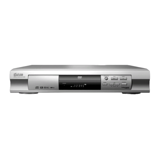
- Page 1 SERVICE MANUAL DVD PLAYER DVP-2003...
-
Page 2: Table Of Contents
TABLE OF CONTENTS SPECIFICATIONS ..............1-1-1 LASER BEAM SAFETY PRECAUTIONS . -
Page 3: Specifications
SPECIFICATIONS ITEM CONDITIONS UNIT NOMINAL LIMIT 1. Video Output 75 ohm load 2. Optical Digital Out 3. Audio (PCM) 3-1. Output Level 1kHz 0dB Vrms 3-2. S/N 3-3. Freq. Response fs=48kHz 20~22kHz ± 2 fs=44.1kHz 20~20 kHz ± 2 3-4. THD+N 1 kHz 0dB 0.005 NOTES:... -
Page 4: Laser Beam Safety Precautions
LASER BEAM SAFETY PRECAUTIONS This DVD player uses a pickup that emits a laser beam. Do not look directly at the laser beam coming from the pickup or allow it to strike against your skin. The laser beam is emitted from the location shown in the figure. When checking the laser diode, be sure to keep your eyes at least 30cm away from the pickup lens when the diode is turned on. -
Page 5: Important Safety Precautions
IMPORTANT SAFETY PRECAUTIONS Product Safety Notice I. Also check areas surrounding repaired locations. J. Be careful that foreign objects (screws, solder Some electrical and mechanical parts have special droplets, etc.) do not remain inside the set. safety-related characteristics which are often not evi- K. -
Page 6: Safety Check After Servicing
Safety Check after Servicing Examine the area surrounding the repaired location for damage or deterioration. Observe that screws, parts, Chassis or Secondary Conductor and wires have been returned to their original posi- tions. Afterwards, do the following tests and confirm the specified values to verify compliance with safety Primary Circuit Terminals standards. -
Page 7: Standard Notes For Servicing
STANDARD NOTES FOR SERVICING Circuit Board Indications How to Remove / Install Flat Pack-IC a. The output pin of the 3 pin Regulator ICs is indi- 1. Removal cated as shown. With Hot-Air Flat Pack-IC Desoldering Machine:. (1) Prepare the hot-air flat pack-IC desoldering Top View Bottom View machine, then apply hot air to the Flat Pack-IC... - Page 8 With Soldering Iron: (4) Bottom of the flat pack-IC is fixed with glue to the CBA; when removing entire flat pack-IC, first apply (1) Using desoldering braid, remove the solder from all soldering iron to center of the flat pack-IC and heat pins of the flat pack-IC.
- Page 9 2. Installation Instructions for Handling Semi-conductors (1) Using desoldering braid, remove the solder from the foil of each pin of the flat pack-IC on the CBA Electrostatic breakdown of the semi-conductors may so you can install a replacement flat pack-IC more occur due to a potential difference caused by electro- easily.
-
Page 10: Cabinet Disassembly Instructions
CABINET DISASSEMBLY INSTRUCTIONS 1. Disassembly Flowchart (1): Identification (location) No. of parts in the figures (2): Name of the part This flowchart indicates the disassembly steps to gain (3): Figure Number for reference access to item(s) to be serviced. When reassembling, (4): Identification of parts to be removed, unhooked, follow the steps in reverse order. - Page 11 (S-1) DVD Mecha [1] Top Cover (S-1) Short the three short lands by soldering (S-1) Fig. D1 Tray Panel (L-2) [3] 5.1CH (L-1) (L-1) View for A Short the three short lands by soldering CN1202 Slide CN1201 (L-3) [2] Front Assembly Fig.
- Page 12 CN1601 (S-4) (S-6) [4] AV CBA CN1001 [6] Rear Panel (S-4) (S-5) (S-3) (S-3) Fig. D6 [5] DVD Main CBA Unit Fig. D5 HOW TO MANUAL EJECT 1. Remove the Top Case. 2. Insert the eject-bar (length = approximately 80 mm, diameter = approximately 3 mm) into the manual eject hole on the DVD Mecha.
-
Page 13: System Control Block Diagram
BLOCK DIAGRAMS System Control Block Diagram IC601 (DVD HOST PROCESSOR) IC301 TFWD (FRONT END PROCESSOR) TREV TFWD TOUT TFWD TREV TREV TOUT +3.3V IC2001 TOUT IC605 (FRONT PANEL CONTROL) FL2001 STDIO FROM/TO STDIO RESET RESET RF SIGNAL GRID PROCESS MUTE 46 MUTE /SERVO HANG... -
Page 14: Block Diagrams
RF Signal Process/Servo Block Diagram DATA(VIDEO/AUDIO) SIGNAL FOCUS SERVO SIGNAL TRACKING SERVO SIGNAL SLIDE SERVO SIGNAL DISK SERVO SIGNAL IC101 (RF SIGNAL PROCESS) PICK-UP UNIT DVD MAIN CBA UNIT HOLD TESTSG CN101 FROM/TO DVD SIGNAL PROCESS BLOCK DIAGRAM NARF C 10 DETECTOR BDO DET INPUT... - Page 15 DVD Signal Process Block Diagram DATA(VIDEO/AUDIO) SIGNAL DVD MAIN CBA UNIT IC201 (DVD SIGNAL PROCESS) PARA0 PARA1 PARA2 DATA VIDEO/AUDIO PARA3 SLICER PARA0-PARA7 TO VIDEO DEMODULATOR FROM/TO RF SIGNAL INTERFACE NARF PARA4 BLOCK DIAGRAM PROCESS/SERVO PARA5 BLOCK DIAGRAM TESTSG PARA6 PARA7 MEMORY MANAGER...
-
Page 16: Video Block Diagram
Video Block Diagram DATA(VIDEO) SIGNAL DATA(AUDIO) SIGNAL VIDEO SIGNAL DATA(VIDEO/AUDIO) SIGNAL IC601 (DVD HOST PROCESSOR) CACHE SUBSYSTEM PCM-MCLK FROM DVD PARA0 INTERNAL CENTRAL FRONT-END PCM-DATA0 SIGNAL PROCESS PARA0-PARA7 PERIPHERALS COMMAND & LINK PCM-DATA1 BLOCK DIAGRAM PARA7 PORTS PORT INTERFACE TO AUDIO PCM-DATA2 AUDIO BLOCK... -
Page 17: Audio Block Diagram
Audio Block Diagram DATA(AUDIO) SIGNAL AUDIO SIGNAL IC1701 (AMP) CN701 CN1601 CN1201 CN1700 CN1701 CN1202 AUDIO(L)-F AUDIO(L)-F AUDIO(L)-SC AUDIO(R)-F AUDIO(R)-F AUDIO(R)-SC AUDIO(L)-R AUDIO(L)-R AUDIO(L)-F IC1700 (AMP) AUDIO(R)-R AUDIO(R)-R AUDIO(R)-F AUDIO-SW AUDIO-SW AUDIO(L)-R JK1404 AUDIO-C AUDIO-C AUDIO(R)-R Q1216, Q1218 AUDIO-SW AUDIO-K MUTE AUDIO-C Q1215, Q1217... -
Page 18: Power Supply Block Diagram
Power Supply Block Diagram CAUTION ! CAUTION Switching power supply circuit is used in this unit. FOR CONTINUED PROTECTION AGAINST FIRE HAZARD, If Main Fuse (F1001) is blown, check to see that all components in the REPLACE ONLY WITH THE SAME TYPE T1.6A L 250V FUSE. power supply circuit are not defective before you connect the AC plug to NOTE : the AC power supply. -
Page 19: Schematic Diagrams / Cba's And Test Points
SCHEMATIC DIAGRAMS / CBA’S AND TEST POINTS Standard Notes Notes: WARNING 1. Do not use the part number shown on these draw- ings for ordering. The correct part number is shown Many electrical and mechanical parts in this chassis in the parts list, and may be slightly different or have special characteristics. - Page 20 LIST OF CAUTION, NOTES, AND SYMBOLS USED IN THE SCHEMATIC DIAGRAMS ON THE FOLLOWING PAGES: 1. CAUTION: FOR CONTINUED PROTECTION AGAINST FIRE HAZARD, REPLACE ONLY WITH THE SAME TYPE FUSE. 2. CAUTION: Fixed Voltage (or Auto voltage selectable) power supply circuit is used in this unit. If Main Fuse (F1001) is blown, first check to see that all components in the power supply circuit are not defec- tive before you connect the AC plug to the AC power supply.
- Page 21 DVD Main 1/4 Schematic Diagram 1-7-3 1-7-4 1-7-5 E56G0SCD1...
- Page 22 DVD Main 2/4 Schematic Diagram 1-7-7 1-7-6 1-7-8 E56G0SCD2...
- Page 23 DVD Main 3/4 Schematic Diagram 1-7-9 1-7-10 1-7-11 E56G0SCD3...
- Page 24 DVD Main 4/4 Schematic Diagram E56G0SCD4 AV 1/4 Schematic Diagram CAUTION ! Switching power supply circuit is used in this unit. If Main Fuse (F1001) is blown, check to see that all components in the power supply circuit are not defective before you connect the AC plug to the AC power supply.
- Page 25 AV 2/4 Schematic Diagram 1-7-15 1-7-16 E56G0SCAV2...
- Page 26 AV 3/4 Schematic Diagram 1-7-17 E56G0SCAV3 1-7-18...
- Page 27 AV 4/4 Schematic Diagram FL2001 MATRIX CHART STANDBY TITLE CHP. TRK. STANDBY REPEAT REPEAT TITLE CHP. TRK. 1-7-19 1-7-20 E56G0SCAV4...
- Page 28 5.1CH Schematic Diagram 1-7-21 1-7-22 E56G0SC51C...
- Page 29 AV CBA Top View NOTE : BECAUSE A HOT CHASSIS GROUND IS PRESENT IN THE POWER CAUTION ! THE VOLTAGE FOR PARTS IN HOT CIRCUIT IS MEASURED USING SUPPLY CIRCUIT, AN ISOLATION TRANSFORMER MUST BE USED. Switching power supply circuit is used in this unit. HOT GND AS A COMMON TERMINAL.
- Page 30 AV CBA Bottom View NOTE : BECAUSE A HOT CHASSIS GROUND IS PRESENT IN THE POWER THE VOLTAGE FOR PARTS IN HOT CIRCUIT IS MEASURED USING CAUTION ! SUPPLY CIRCUIT, AN ISOLATION TRANSFORMER MUST BE USED. Switching power supply circuit is used in this unit. HOT GND AS A COMMON TERMINAL.
- Page 31 5.1CH CBA Top View 5.1CH CBA Bottom View 1-7-27 1-7-28 BE56G0F02021...
-
Page 32: Waveforms
WAVEFORMS Pin 8 of CN1601 Pin 18 of CN1601 NOTE: Input CD: 1kHz PLAY (WF4~WF6) DVD: POWER ON (STOP) MODE (WF1~WF3) VIDEO-Y 0.2V 20usec AUDIO(R)-F 0.5msec Pin 10 of CN1601 Pin 21 of CN1601 VIDEO-CVBS 0.5V 20usec SPDIF 0.2usec Pin 12 of CN1601 VIDEO-C 0.2V 20usec... -
Page 33: Wiring Diagram
WIRING DIAGRAM FRONT SPEAKER REAR SPEAKER VIDEO AUDIO AUDIO AUDIO AUDIO SUB- CENTER DIGITAL OPTICAL S-VIDEO AC CORD OUT(L) OUT(R) OUT(L) OUT(R) WOOFER SPEAKER AUDIO OUT AUDIO OUT SCART JACK CN1202 CN1701 AUDIO(L)-SC AUDIO(R)-SC AUDIO(L)-F AUDIO(R)-F AV CBA (BE56G0F01011) AUDIO(L)-R AUDIO(R)-R AUDIO-SW AUDIO-C... -
Page 34: Firmware Renewal Mode
FIRMWARE RENEWAL MODE 1. Turn the power on and remove the disc on the tray. 2. To put the DVD player into version up mode, press [9], [8], [7], [6], and [SEARCH MODE] buttons on the remote control unit in that order. The tray will open automatically. -
Page 35: System Control Timing Charts
SYSTEM CONTROL TIMING CHARTS Tray close ~ Play / Play ~ Tray open Eject key on Eject key on Tray close Play Tray open Disc Rotation LSW2 LSW1 4.4s (TL123) 700ms 2.0s 1.2s ( TP122 ) 1.7s ( TL122 ) 1-11-1 E5638TI... -
Page 36: Ic Pin Function Descriptions
IC PIN FUNCTION DESCRIPTIONS IC2001 [ PT6315-S/ PT6315-S(-TP) ] Signal In/Out Name Function Name Clock Input Serial Interface Strobe Key Data 1 Input Key Data 2 Input Power Supply a / KEY-1 Segment Output / Key Source-1 Segment Output / Key b / Key-2 Source-2 Segment Output / Key... -
Page 37: Lead Identifications
LEAD IDENTIFICATIONS FS1KM-18A 2SC2785 (H) 2SA1015-Y (TPE2) KTC3199 (GR) 2SC2236-Y-TPE6,C KRA110M 2SA966(Y) KRC110M-AT KTC3205 (Y) BA1L3Z-T BN1L3Z (P) KTA1273(Y) KTA1266 (GR) G D S E C B E C B PQ018EF01SZ PT6315-S KIA431-AT PT6315-S(-TP) NJM2058D R A K 0C-0805T-002 GP1FA512TZV MM1567AJ LTV-817B-F LTV-817C-F... -
Page 38: Exploded Views
EXPLODED VIEWS Cabinet 2L011 2L011 See Electrical Parts List for parts with this mark. Some Ref. Numbers are not in sequence. 2L021 2L021 2L021 2L031 2L011 2L100 W1601 JK1401 JK1402 JW001 JK1404 JK1403 DVD Main JK1202 W1001 CBA Unit IC1204 2L031 5.1CH CBA 2L031... - Page 39 Packing Unit 1-14-2 E56G0EX...
-
Page 40: Mechanical Parts List
MECHANICAL PARTS LIST PRODUCT SAFETY NOTE: Products marked with a ! have special characteristics important to safety. Before replacing any of these components, read care- fully the product safety notice in this service manual. Don't degrade the safety of the product through improper servicing. -
Page 41: Electrical Parts List
ELECTRICAL PARTS LIST PRODUCT SAFETY NOTE: Products marked with a Ref. No. Description Part No. ! have special characteristics important to safety. C1039 ELECTROLYTIC CAP. 47µF/16V M CE1CMASDL470 Before replacing any of these components, read care- C1040 ELECTROLYTIC CAP. 100µF/6.3V M CE0KMASDL101 fully the product safety notice in this service manual. - Page 42 Ref. No. Description Part No. Ref. No. Description Part No. CHIP CERAMIC CAP. B K 0.1µF/16V CHD1CK30B104 D1050 ZENER DIODE DZ-6.2BSBT265 or NDTB0DZ6R2BS CONNECTORS ZENER DIODE MTZJT-776.2B QDTB0MTZJ6R2 D1051 RECTIFIER DIODE 1N4005 or NDQZ001N4005 CN1001 FMN CONNECTOR, TOP 26P 26FMN-BTRK JCFNG26JG002 RECTIFIER DIODE 1N4005 ND8Z001N4005...
- Page 43 Ref. No. Description Part No. Ref. No. Description Part No. L1001! LINE FILTER 50MH LF-4Z-E503 or LLBG00ZKQ008 TRANSISTOR 2SC2785(H) QQSH02SC2785 LINE FILTER 50MH LF-4D-E503 or LLBG00ZKQ009 Q1213 TRANSISTOR KTA1266(Y) or NQSY0KTA1266 LINE FILTER 58MH ELF15N902AN LLBG00ZMS035 TRANSISTOR 2SA1015-Y(TPE2) QQSY02SA1015 L1002 PCB JUMPER D0.6-P5.0 JW5.0T Q1214...
- Page 44 Ref. No. Description Part No. Ref. No. Description Part No. CARBON RES. 1/4W J 1k Ω CHIP RES.(1608) 1/16W J 100k Ω RCX4JATZ0102 RRXGJR5Z0104 CARBON RES. 1/6W J 100k Ω or CHIP RES.(1608) 1/10W J 100k Ω or R1036 RCX6JATZ0104 R1240 RRXAJR5Z0104 CARBON RES.
- Page 45 Ref. No. Description Part No. Ref. No. Description Part No. CHIP RES.(1608) 1/16W J 1.6k Ω CHIP RES.(1608) 1/16W J 8.2k Ω RRXGJR5Z0162 RRXGJR5Z0822 CHIP RES.(1608) 1/10W J 2.2k Ω or CHIP RES.(1608) 1/10W J 47k Ω or R1353 RRXAJR5Z0222 R1526 RRXAJR5Z0473 CHIP RES.(1608) 1/16W J 2.2k Ω...
- Page 46 Ref. No. Description Part No. Ref. No. Description Part No. CERAMIC CAP.(AX) B K 1000pF/50V or CCA1JKT0B102 C1721 CHIP CERAMIC CAP. CH J 560pF/50V CHD1JJ3CH561 CERAMIC CAP.(AX) CH J 1000pF/50V CA1J102TU008 C1722 ELECTROLYTIC CAP. 10µF/25V M CE1EMASDL100 JK1202 RCA JACK(BLACK) MSP-251V-01 PBSN JXRL010LY059 C1723 ELECTROLYTIC CAP.
- Page 47 Ref. No. Description Part No. Ref. No. Description Part No. CHIP RES.(1608) 1/16W F 1.5k Ω or CHIP RES.(1608) 1/10W J 1k Ω R1714 RRXGFR5Z0152 R1764 RRXAJR5Z0102 CHIP RES.(1608) 1/10W F 1.5k Ω CHIP RES.(1608) 1/10W 0 Ω RRXAFR5Z1501 R1773 RRXAZR5Z0000 CHIP RES.(1608) 1/16W F 1.8k Ω...