Table of Contents
Advertisement
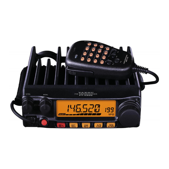
FM TRANSCEIVER
FT-2900R
Technical Supplement
©2009 VERTEX STANDARD CO., LTD.
Introduction
This manual provides technical information necessary for servicing the FT-2900R FM Transceiver.
Servicing this equipment requires expertise in handling surface-mount chip components. Attempts by non-
qualified persons to service this equipment may result in permanent damage not covered by the warranty,
and may be illegal in some countries.
Two PCB layout diagrams are provided for each double-sided circuit board in the Transceiver. Each side of is
referred to by the type of the majority of components installed on that side ("leaded" or "chip-only"). In most
cases one side has only chip components, and the other has either a mixture of both chip and leaded compo-
nents (trimmers, coils, electrolytic capacitors, ICs, etc.), or leaded components only.
While we believe the technical information in this manual to be correct, VERTEX STANDARD assumes no
liability for damage that may occur as a result of typographical or other errors that may be present. Your
cooperation in pointing out any inconsistencies in the technical information would be appreciated.
The transceiver was assembled using Pb (lead) free solder, based on the RoHS specification.
Only lead-free solder (Alloy Composition: Sn-3.0Ag-0.5Cu) should be used for repairs performed on this appara-
tus. The solder stated above utilizes the alloy composition required for compliance with the lead-free specification,
and any solder with the above alloy composition may be used.
Specifications ...................................................... 2
Exploded View & Miscellaneous Parts ............ 3
Block Diagram .................................................... 5
Connection Diagram .......................................... 6
Circuit Description ............................................. 7
Alignment ............................................................ 9
VERTEX STANDARD CO., LTD.
4-8-8 Nakameguro, Meguro-Ku, Tokyo 153-8644, Japan
VERTEX STANDARD
US Headquarters
10900 Walker Street, Cypress, CA 90630, U.S.A.
YAESU UK LTD.
Unit 12, Sun Valley Business Park, Winnall Close
Winchester, Hampshire, SO23 0LB, U.K.
VERTEX STANDARD HK LTD.
Unit 5, 20/F., Seaview Centre, 139-141 Hoi Bun Road,
Kwun Tong, Kowloon, Hong Kong
VERTEX STANDARD ( AUSTRALIA ) PTY., LTD.
Normanby Business Park, Unit 14/45 Normanby Road
EH039N90A
Notting Hill 3168, Victoria, Australia
Important Note
Contents
Board Unit
MAIN Unit Circuit Diagram ................................. 13
MAIN Unit Parts Layout ....................................... 15
MAIN Unit Parts List ............................................ 17
CNTL Unit Circuit Diagram ................................. 27
CNTL Parts Layout ............................................... 28
CNTL Parts List .................................................... 29
(Schematics, Layouts & Parts)
1
Advertisement
Table of Contents

Related Manuals for Yaesu FT-2900R


Summary of Contents for Yaesu FT-2900R
-
Page 1: Table Of Contents
Notting Hill 3168, Victoria, Australia Introduction This manual provides technical information necessary for servicing the FT-2900R FM Transceiver. Servicing this equipment requires expertise in handling surface-mount chip components. Attempts by non- qualified persons to service this equipment may result in permanent damage not covered by the warranty, and may be illegal in some countries. -
Page 2: Specifications
Specifications General Frequency Range: Tx 144 - 146 MHz or 144 - 148 MHz Rx 144 - 146 MHz or 136 - 174 MHz Channel Step: 5/10/12.5/15/20/25/50/100 kHz Standard Repeater Shift: ±600 kHz Frequency Stability: Better than ±10 ppm [–4 °F to +140 °F (–20 °C to +60 °C)] Modes of Emission: F2D/F3E Antenna Impedance:... -
Page 3: Exploded View & Miscellaneous Parts
Exploded View & Miscellaneous Parts ACCESSORIES VXSTD P/N DESCRIPTION MICROPHONE ( MH-48 AAA43X001 T9025825 DC CABLE SPARE FUSE ( 25 A ) Q0000074 FOOT S8002050 BRACKET ( MMB-83 ) RA1119800 REF. VXSTD P/N DESCRIPTION QTY. U03310002 SEMS SCREW ASM3X10NI P1091172 U24310001 BIND HEAD TAPTITE-B M3X10 CONNECTOR... - Page 4 Note...
-
Page 5: Block Diagram
Block Diagram... -
Page 6: Connection Diagram
Connection Diagram... -
Page 7: Circuit Description
Circuit Description Receive Signal Path The audio signal passes through a band-pass filter consisting of Q1046 and Q1047 (both 2SC4081), and Incoming RF signal is from the antenna jack is deliv- the audio mute gate Q1039 (2SJ347), to the audio ered to the Main Unit and passed through the low- VR which adjusts the audio sensitivity to compen- pass filter network consisting capacitors C1213,... - Page 8 Circuit Description TX APC Circuit The 21.25 MHz frequency of the reference oscillator circuit made up of X1001 is divided by the reference A portion of the power amplifier module output is frequency divider section of Q1011 (MB15A01PFV1) rectified by D1022 (1SS321), then delivered to APC into 4250 or 3400 parts to become 5 kHz or 6.25 kHz Q1038 (LM2904PWR), as a DC voltage which is pro- comparative reference frequencies, which are uti-...
-
Page 9: Alignment
Alignment Introduction Required Test Equipment The FT-2900R is carefully aligned at the factory for The following test equipment (and familiarity with the specified performance across the amateur band. its use) is necessary for complete realignment. Cor- Realignment should therefore not be necessary ex- rection of problems caused by misalignment result- cept in the event of a component failure. -
Page 10: Test Setup
B0111 tL B0111 tL.” eter to “B0111 tL B0111 tL Alignment of the FT-2900R is performed using a front Press the [ D/MR ( MW )] key to enable adjustment panel software-based procedure. To perform align- of the “Squelch Threshold Level.”... - Page 11 Alignment S-meter Level (S-1) TX Power (Low 2) Rotate the DIAL knob to set the alignment param- Inject a 145.100 MHz signal at a level of –5 dBµ eter to “B0101 L2 B0101 L2 B0101 L2 B0101 L2.” B0101 L2 (with 1 kHz modulation @±3.5 kHz deviation) Press the [ D/MR ( MW )] key to enable adjustment from the RF signal generator.
- Page 12 Alignment DCS TX Deviation Rotate the DIAL knob to set the alignment param- Closing the Alignment mode eter to “B0101 dC B0101 dC B0101 dC B0101 dC B0101 dC.” 1. Press the [DW(REV)] key to save the new setting and Press the [ D/MR ( MW )] key to enable adjustment exit to normal operation.
-
Page 13: Main Unit Circuit Diagram
MAIN Unit Circuit Diagram Low 1 : 0.0 V (2.8 V) Low 2 : 0.0 V (3.0 V) Low 3 : 0.0 V (3.3 V) HIGH : 0.0 V (4.0 V) 4.3 V (4.3 V) 3.3 V (3.3 V) 4.0 V (4.0 V) 6.2 V (4.5 V) 0.0 V (1.6 V) 4.9 V (4.9 V) - Page 14 MAIN Unit Note...
-
Page 15: Main Unit Parts Layout
MAIN Unit Parts Layout (Side A) S-AV36A KIA7808API (Q1030) (Q1015) 2SA1774 (FR) 2SJ615 (Q1007) (Q1008) CD4094BPWR 2SK296ZQ (ZQ) (Q1048) (Q1037, 1045) MB15A01PFV1 (Q1011) NJM2591V (Q1028) DTC143ZE (E23) DTC144EE (26) (Q1054) (Q1003, 1004, 1014) DTC143EE (23) (Q1052) DA221 (26) DAN235E (M) (D1011, 1013, 1016) (D1010) 2SC4081 (B) -
Page 16: Main Unit
MAIN Unit Parts Layout (Side B) LM2902PWR M62364FP LM2904PWR (Q1005, 1049) (Q1043) (Q1006, 1038, 1044, 1050) 2SA1774 (FR) 2SJ347 (KS) 2SJ364 (4M) (Q1024, 2027, 1029) (Q1039) (Q1034, 1036, 1041, 1042) 2SC4081 (B) DTC144EE (26) S-812C50AUA (Q1001, 1012, 1021, (Q1013, 1018, 1019, (Q1016) 1046, 1047) 1020, 1031, 1040) -
Page 17: Main Unit Parts List
MAIN Unit Parts List DESCRIPTION VALUE TOL. MFR'S DESIG VXSTD P/N VERS. LOT SIDE LAY ADR PCB with Components CS2040501 Printed Circuit Board FR020070C C 1001 CHIP TA.CAP. 10uF TAJA106M010Y K78100072 C 1002 CHIP TA.CAP. 10uF TAJA106M010Y K78100072 C 1003 CHIP CAP. -
Page 18: Parts List
MAIN Unit Parts List DESCRIPTION VALUE TOL. MFR'S DESIG VXSTD P/N VERS. LOT SIDE LAY ADR C 1079 CHIP CAP. 150pF GRM1882C1H151JA01D K22174239 C 1080 CHIP CAP. 560pF GRM1882C1H561JA01D K22174273 C 1081 CHIP CAP. 0.001uF GRM188B11H102KA01D K22174821 C 1082 AL.ELECTRO.CAP. 100uF USR1C101MDD K40129110... - Page 19 MAIN Unit Parts List DESCRIPTION VALUE TOL. MFR'S DESIG VXSTD P/N VERS. LOT SIDE LAY ADR C 1162 CHIP CAP. 0.001uF GRM188B11H102KA01D K22174821 C 1163 AL.ELECTRO.CAP. 10uF UWX1C100MCL1GB K48120026 C 1164 CHIP TA.CAP. 4.7uF TAJA475M016Y K78120079 C 1165 CHIP CAP. 0.001uF GRM188B11H102KA01D K22174821...
- Page 20 MAIN Unit Parts List DESCRIPTION VALUE TOL. MFR'S DESIG VXSTD P/N VERS. LOT SIDE LAY ADR C 1249 CHIP CAP. GRM1884C1H1R0BZ01D K22174267 C 1250 CHIP CAP. 22pF GRM1882C1H220JA01D K22174219 C 1251 CHIP CAP. GRM1884C1H1R0BZ01D K22174267 C 1252 CHIP CAP. 39pF GRM1882C1H390JA01D K22174225 C 1253...
- Page 21 MAIN Unit Parts List DESCRIPTION VALUE TOL. MFR'S DESIG VXSTD P/N VERS. LOT SIDE LAY ADR FB1002 FERRITE BEADS SMB304729 L9190094 FB1003 FERRITE BEADS SMB304729 L9190094 FB1004 FERRITE BEADS SMB304729 L9190094 FB1005 FERRITE BEADS SMB304729 L9190094 FB1006 FERRITE BEADS BLM18PG330SN1D L9190141 FB1007 FERRITE BEADS...
- Page 22 MAIN Unit Parts List DESCRIPTION VALUE TOL. MFR'S DESIG VXSTD P/N VERS. LOT SIDE LAY ADR Q 1044 LM2904PWR G1094010 Q 1045 3SK296ZQ-TL-E G4802968 Q 1046 TRANSISTOR 2SC4081 T106 R G3340818R Q 1047 TRANSISTOR 2SC4081 T106 R G3340818R Q 1048 CD4094BPWR G1093866 Q 1049...
- Page 23 MAIN Unit Parts List DESCRIPTION VALUE TOL. MFR'S DESIG VXSTD P/N VERS. LOT SIDE LAY ADR R 1067 CHIP RES. 390k 1/16W RMC1/16S 394JTH J24189056 R 1068 CHIP RES. 100k 1/16W RMC1/16S 104JTH J24189049 R 1069 CHIP RES. 100k 1/16W RMC1/16S 104JTH J24189049 R 1070...
- Page 24 MAIN Unit Parts List DESCRIPTION VALUE TOL. MFR'S DESIG VXSTD P/N VERS. LOT SIDE LAY ADR R 1146 CHIP RES. RMC1 820JTE J24305820 R 1147 CHIP RES. 220k 1/16W RMC1/16S 224JTH J24189053 R 1148 CHIP RES. 1/16W RMC1/16S 103JTH J24189037 R 1149 CHIP RES.
- Page 25 MAIN Unit Parts List DESCRIPTION VALUE TOL. MFR'S DESIG VXSTD P/N VERS. LOT SIDE LAY ADR R 1224 CHIP RES. 330k 1/16W RMC1/16S 334JTH J24189055 R 1225 CHIP RES. 330k 1/16W RMC1/16S 334JTH J24189055 R 1226 CHIP RES. 5.6k 1/16W RMC1/16S 562JTH J24189034 R 1228...
- Page 26 MAIN Unit Note...
-
Page 27: Cntl Unit Circuit Diagram
CNTL Unit Circuit Diagram 3.5 V (3.5 V) 2.3 V (2.3 V) 5.0 V (5.0 V) 5.0 V (5.0 V) 5.0 V (5.0 V) 3.8 V (3.8 V) Q 2001 3.3 V Note (3.3 V) 0.0 V 4.0 Vp-p TONE ON 5.0 V (5.0 V) 0.0 V 5.0 Vp-p DCS ON... -
Page 28: Cntl Parts Layout
CNTL Unit Parts Layout HD64F2266TF13 BR24L64 (Q2001) (Q2005) 2SC4617 (BR) BD4830FVE (Q2006, 2007, 2012) (Q2010) 2SC5374 (NA) (Q2002) S-812C50AUA DTC143ZE (E23) (Q2009) (Q2003) (Side A) CPH6202 (CB) (Q2004) DA221 (26) DAN222 (N) (D2001, 2025) (D2024) (Side B) -
Page 29: Cntl Parts List
CNTL Unit Parts List DESCRIPTION VALUE TOL. MFR'S DESIG VXSTD P/N VERS. LOT SIDE LAY ADR PCB with Components Printed Circuit Board FR020080C C 2001 CHIP CAP. 0.001uF GRM155B11H102KA01D K22178809 C 2002 CHIP CAP. 0.001uF GRM155B11H102KA01D K22178809 C 2003 CHIP CAP. 0.001uF GRM155B11H102KA01D K22178809... - Page 30 CNTL Unit Parts List DESCRIPTION VALUE TOL. MFR'S DESIG VXSTD P/N VERS. LOT SIDE LAY ADR D 2011 SML-512WWT86 G2071104 D 2012 SML-512WWT86 G2071104 D 2013 SML-512WWT86 G2071104 D 2014 DIODE 1SS400 TE61 G2070634 D 2015 DIODE 1SS400 TE61 G2070634 D 2016 DIODE 1SS400 TE61...
- Page 31 CNTL Unit Parts List DESCRIPTION VALUE TOL. MFR'S DESIG VXSTD P/N VERS. … LAY ADR R 2037 CHIP RES. 390k 1/16W 0.5% MCR01MZPD3903 J24189331 R 2038 CHIP RES. 1/16W 0.5% MCR01MZPD1002 J24189374 R 2040 CHIP RES. RMC1 100JTE J24305100 R 2042 CHIP RES.
- Page 32 CNTL Unit Note...
- Page 34 Copyright 2009 VERTEX STANDARD CO., LTD. All rights reserved No portion of this manual may be reproduced without the permission of VERTEX STANDARD CO., LTD. Printed in Japan.