Table of Contents
Advertisement
SERVICE MANUAL
System
Power Amplifier: Pure-complementary SEPP MOS FET power
amplifier with all stages directly coupled
Preamplifier: Low-noise, high-gain equalizer amplifier
Power section: Large-capacity power supply advanced STD
Rated output
4 ohms, 120 W + 120 W (DIN 0.7%, 1 kHz)
8 ohms, 80 W + 80 W (DIN 0.7%, 1 kHz)
Speaker Impedance
4 to 16 ohms
Output bandwidth (8 ohms)
10 Hz to 100 kHz (at 40 W output, and high-frequency distortion
rate of 0.08%)
Total harmonic distortion
0.008% (at 8 ohms, 10 W output)
Damping factor
100 (8 ohms, 1 kHz)
Intermodulation (1M) distortion (60 Hz : 7 kHz = 4 : 1)
0.008% (8 ohms)
Throughrate
125 V/µ sec, 250 V/µ sec (Inside)
Residual noise
Less than 100 µV (network A)
Equalizer deviation
PHONO MM: 20 Hz to 20 kHz, ± 5 dB
Frequency response
TUNER, CD, AUX, TAPE1/DAT, TAPE2/MD: 7 Hz to
+0
100 kHz
dB
– 3
S/N
PHONO MC: 78 dB (network A, 0.5 mV)
MM: 95 dB (network A, 5 mV)
TUNER, CD, AUX, TAPE1/DAT, TAPE2/MD: 105 dB
MICROFILM
TA-FA30ES
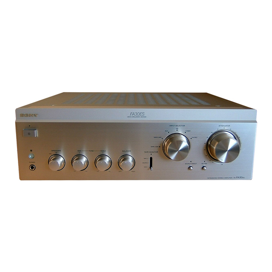
Photo: GOLD model
SPECIFICATIONS
Inputs
Input sensitivity and impedance
PHONO MC: 0.17 mV, 100 ohms
MM: 2.5 mV, 50 kilohms
TUNER, CD, AUX, TAPE1/DAT, TAPE2/MD: 150 mV,
20 kilohms
Maximum input capability (1 kHz)
PHONO MC: 9 mV
MM: 150 mV
Outputs
Output level/impedance
REC OUT 1, 2: 150 mV, 1 kilohm
PHONES: 10 mW (at 8 ohms)
Tone controls
BASS (100 Hz): ± 7 dB
TREBLE (10 kHz): ± 7 dB
General
Power requirements
230 V AC, 50/60 Hz
Power consumption
220 W
Dimensions (approx) (w/h/d)
430
150
415 mm incl. projecting parts and controls
Mass (approx)
11.0 kg
Supplied accessories
Remote commander (remote ) RM-S326 (1)
Sony batteries R6 (size-AA) (2)
Design and specifications are subject to change without notice.
INTEGRATED STEREO AMPLIFIER
AEP Model
UK Model
E Model
Australian Model
Chinese Model
Advertisement
Table of Contents

Related Manuals for Sony TA-FA30ES


Summary of Contents for Sony TA-FA30ES
-
Page 1: Service Manual
PHONO MM: 20 Hz to 20 kHz, ± 5 dB Supplied accessories Remote commander (remote ) RM-S326 (1) Frequency response Sony batteries R6 (size-AA) (2) TUNER, CD, AUX, TAPE1/DAT, TAPE2/MD: 7 Hz to 100 kHz – 3 Design and specifications are subject to change without notice. -
Page 2: Table Of Contents
LINE WITH MARK ! ON THE SCHEMATIC DIAGRAMS AND IN THE PARTS LIST ARE CRITICAL TO SAFE OPERATION. REPLACE THESE COMPONENTS WITH SONY PARTS WHOSE PART NUMBERS APPEAR AS SHOWN IN THIS MANUAL OR IN SUPPLEMENTS PUB- LISHED BY SONY. -
Page 3: General
SECTION 1 GENERAL LOCATION OF CONTROLS Front Panel 1 U (Power) switch and indicator 2 TAPE MONITOR switch and indicator 3 INPUT SELECTOR switch and indicator 4 ATTENUATOR control 5 PHONES jack 6 Remote control sensor 7 SPEAKERS switch 8 BASS control 9 TREBLE control !º... -
Page 4: Disassembly
SECTION 2 DISASSEMBLY Note: Follow the disassembly procedure in the numerical order given. CASE, FRONT PANEL 1 two screws 1 screw (CASE 3 TP2) (CASE 3 TP2) 2 case (413235) 1 two screws (CASE 3 TP2) 5 three screws 1 two screws 6 front panel (CASE 3 TP2) 3 knob (SEL) - Page 5 MAIN BOARD 5 three screws 5 four screws 2 connector (CN752) 6 four screws 4 three screws (BV/RING) 5 four screws 3 connector (CN104) 7 main board 1 connector (CN751) – 5 –...
-
Page 6: Electrical Adjustments
SECTION 3 ELECTRICAL ADJUSTMENTS Bias Adjustment 1. Rotate fully the bias adjusting semi-fixed resistors (RV500, RV600) to the MIN position (counterclockwise). 2. Connect a digital voltmeter to the CN500 and CN600. 1 pin 3 pin CN500 – CN600 – 3. Set the slidack to 0 V, and press the U button (ON) on the set. -
Page 7: Diagrams
SECTION 4 DIAGRAMS • Circuit Boards Location 4-1. NOTE FOR PRINTED WIRING BOARDS AND SCHEMATIC DIAGRAMS (In addition to this, the necessary note is printed in each block.) Note on Schematic Diagram: Note on Printed Wiring Boards: • All capacitors are in µF unless otherwise noted. pF: µµF •... - Page 8 TA-FA30ES 4-2. PRINTED WIRING BOARDS – INPUT Section – • See page 7 for circuit Boards Location. • Semiconductor Location (Page 14) Ref. No. Location Ref. No. Location D101 Q100 D103 Q101 D104 Q102 D105 Q103 D106 Q104 D107 Q105...
-
Page 9: Schematic Diagram - Input Section
TA-FA30ES 4-3. SCHEMATIC DIAGRAM – INPUT Section – (Page 16) (Page 19) (Page 20) – 11 – – 12 –... -
Page 10: Printed Wiring Boards - Main Section
TA-FA30ES (Page 9) 4-4. PRINTED WIRING BOARDS – MAIN Section – • See page 7 for Circuit Boards Location. (Page 18) (Page 17) (Page 18) (Page 22) • Semiconductor Location Ref. No. Location Ref. No. Location Ref. No. Location Ref. No. Location... -
Page 11: Schematic Diagram – Main Section
TA-FA30ES 4-5. SCHEMATIC DIAGRAM – MAIN Section – • See page 25 for IC Block Diagram. (Page 20) (Page 19) (Page 11) (Page 19) (Page 24) (Page 24) The components identified by mark ! or dotted line with mark ! are critical for safety. -
Page 12: Printed Wiring Boards - Panel Section
TA-FA30ES 4-6. PRINTED WIRING BOARDS – PANEL Section – • See page 7 for Circuit Boards Location. (Page 10) (Page 13) • Semiconductor Location – PANEL Board – Ref. No. Location D901 D902 D903 D904 D905 D906 D907 D908 B-11... -
Page 13: Schematic Diagram - Panel Section
TA-FA30ES 4-7. SCHEMATIC DIAGRAM – PANEL Section – • See page 25 for IC Block Diagram. • Waveform 1 IC901 #™ (XOUT) 4.4 Vp-p 8 MHz (Page 16) (Page 15) (Page 16) (Page 11) (Page 11) – 19 – – 20 –... -
Page 14: Printed Wiring Boards – Power Section
TA-FA30ES 4-8. PRINTED WIRING BOARDS – POWER Section – • See page 7 for Circuit Boards Location. (Page 14) (Page 14) – 21 – – 22 –... -
Page 15: Schematic Diagram - Power Section
TA-FA30ES 4-9. SCHEMATIC DIAGRAM – POWER Section – (Page 16) (Page 15) The components identified by mark ! or dotted line with mark ! are critical for safety. Replace only with part number specified. – 23 – – 24 –... -
Page 16: 4-10. Ic Pin Function Description
• IC Block Diagrams 4-10. IC PIN FUNCTION DESCRIPTION PANEL BOARD IC901 TMP47C200BN-H351 (SYSTEM CONTROLLER) IC700 µPC1237HA (SP TM BOARD) Pin No. Pin Name Function Serial clock signal output to the EEPROM (IC902) OVER LOAD DET Two-way data bus with the EEPROM (IC902) MUTE Volume motor drive signal output to the BA6208 (IC903) (for volume down direction) OFFSET DET... -
Page 17: Exploded Views
4-999-428-01 PANEL, FRONT (BLACK) 4-999-432-11 KNOB (VOL) (GOLD) 4-999-428-11 PANEL, FRONT (GOLD) 4-999-430-01 BASE (R), PANEL (BLACK) 4-942-568-41 EMBLEM (NO.5), SONY (BLACK) 4-999-430-11 BASE (R), PANEL (GOLD) 4-942-568-51 EMBLEM (NO.5), SONY (GOLD) 4-210-291-01 SCREW (CASE 3 TP2) (BLACK) X-4950-462-1 LENS ASSY, LED... - Page 18 (2) FRONT PANEL SECTION-2 not supplied supplied supplied with J800 supplied supplied supplied with S903 Supplied with S901, RV303, RV302, RV301 supplied with RV304 The components identified by mark ! or dotted line with mark ! are critical for safety. Replace only with part number specified.
- Page 19 (3) CHASSIS SECTION-1 supplied supplied supplied supplied supplied supplied supplied The components identified by mark ! or dotted line with mark ! are critical for safety. Replace only with part number specified. Ref. No. Part No. Description Remark Ref. No. Part No.
- Page 20 (4) CHASSIS SECTION-2 supplied supplied supplied supplied CNP1 supplied supplied not supplied not supplied supplied supplied supplied supplied not supplied The components identified by mark ! or dotted line with mark ! are critical for safety. Replace only with part number specified. Ref.
-
Page 21: Electrical Parts List
SECTION 6 INPUT ELECTRICAL PARTS LIST NOTE: • Due to standardization, replacements in the • Items marked “*” are not stocked since they The components identified by mark ! or dotted line with mark are seldom required for routine service. parts list may be different from the parts speci- ! are critical for safety. - Page 22 INPUT MAIN Ref. No. Part No. Description Remark Ref. No. Part No. Description Remark C613 1-136-163-00 FILM 0.068uF RY106 1-515-614-11 RELAY C617 1-126-023-11 ELECT 100uF RY107 1-515-614-11 RELAY RY108 1-515-614-11 RELAY C712 1-128-552-51 ELECT 47uF C713 1-126-933-11 ELECT 100uF ************************************************************ C714 1-126-964-11 ELECT 10uF...
- Page 23 MAIN PANEL Ref. No. Part No. Description Remark Ref. No. Part No. Description Remark Q512 8-729-015-31 FET 2SJ201-Y R610 1-259-183-11 CARBON 4.7K 1/4W Q513 8-729-140-84 TRANSISTOR 2SC1841-PAFAEA ! R611 1-249-405-11 CARBON 1/4W F Q600 8-729-045-15 TRANSISTOR 2SC5169-FG R612 1-259-183-11 CARBON 4.7K 1/4W Q601...
- Page 24 PANEL PHONO Ref. No. Part No. Description Remark Ref. No. Part No. Description Remark D906 8-719-911-19 DIODE 1SS119 R917 1-249-429-11 CARBON 1/4W D907 8-719-911-19 DIODE 1SS119 R918 1-249-429-11 CARBON 1/4W D908 8-719-911-19 DIODE 1SS119 R919 1-249-429-11 CARBON 1/4W D910 8-719-986-56 DIODE HZS24-3LTA D911 8-719-200-82 DIODE 11ES2 R920...
- Page 25 PHONO POWER LED Ref. No. Part No. Description Remark Ref. No. Part No. Description Remark C252 1-101-880-00 CERAMIC 47PF < SWITCH > C253 1-106-359-00 MYLAR 4700PF 200V S101 1-762-395-11 SWITCH, PUSH (1 KEY) (PHONO CARTRIDGE) C254 1-126-024-11 ELECT 220uF ************************************************************ C255 1-130-341-00 FILM 0.056uF...
- Page 26 TA-FA30ES SP TM Ref. No. Part No. Description Remark Ref. No. Part No. Description Remark A-4407-670-A SP TM BOARD, COMPLETE RY503 1-515-920-11 RELAY (24V) ********************** < TERMINAL > < CAPACITOR > TM501 1-537-235-11 TERMINAL BOARD (SP) C700 1-126-965-11 ELECT 22uF...