Table of Contents
Advertisement
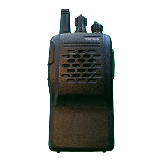
VX-210AU
UHF Band
Service Manual
©2002 VERTEX STANDARD CO., LTD. Printed in Japan.
Operating Manual Reprint ......................................................................................................................................... 2
Specifications ............................................................................................................................................................... 5
Cloning.......................................................................................................................................................................... 6
Exploded View & Miscellaneous Parts ..................................................................................................................... 7
Block Diagram .............................................................................................................................................................. 8
Circuit Description ...................................................................................................................................................... 9
Alignment ................................................................................................................................................................... 11
Board Units (Schematics, Layouts & Parts)
MAIN Unit ............................................................................................................................................................. 13
SW Unit ................................................................................................................................................................... 37
Optional Board Units (Schematics, Layouts & Parts)
VTP-50 VX-Trunk Unit .......................................................................................................................................... 38
FVP-25 Encryption / DTMF Pager Unit ................................................................................................................ 40
VERTEX STANDARD CO., LTD.
4-8-8 Nakameguro, Meguro-Ku, Tokyo 153-8644, Japan
VERTEX STANDARD
US Headquarters
10900 Walker Street, Cypress, CA 90630, U.S.A.
International Division
8350 N.W. 52nd Terrace, Suite 201, Miami, FL 33166, U.S.A.
YAESU EUROPE B.V.
P.O. Box 75525, 1118 ZN Schiphol, The Netherlands
YAESU UK LTD.
Unit 12, Sun Valley Business Park, Winnall Close
Winchester, Hampshire, SO23 0LB, U.K.
VERTEX STANDARD HK LTD.
Unit 5, 20/F., Seaview Centre, 139-141 Hoi Bun Road,
Kwun Tong, Kowloon, Hong Kong
EC020U90A
Introduction
The Vertex VX-210AU is a compact hand portable trans-
ceiver for the UHF land mobile band that offers the conve-
nience of small size, light weight, and simple operation.
The VX-210AU can be simply programmed by your
Vertex Dealer with up to 16 channels for single and split
frequency operation. The VX-210AU provides up to 5
watts of RF output power and includes a flexible quick-
connect antenna.
The transceiver and Ni-Cd battery packs are construct-
ed of thick high-impact polycarbonate plastic, with spe-
cial attention paid by the designers to tight seals and rug-
gedness, assuring years of reliable operation even in harsh
environments.
The following pages describe the operation, features
and accessories of the VX-210AU. With proper care and
operation, the transceiver will provide many years of re-
liable communications.
Contents
1
Advertisement
Table of Contents

Related Manuals for Vertex Standard VX-210AU


Summary of Contents for Vertex Standard VX-210AU
-
Page 1: Table Of Contents
Kwun Tong, Kowloon, Hong Kong EC020U90A Introduction The Vertex VX-210AU is a compact hand portable trans- ceiver for the UHF land mobile band that offers the conve- nience of small size, light weight, and simple operation. The VX-210AU can be simply programmed by your Vertex Dealer with up to 16 channels for single and split frequency operation. -
Page 2: Operating Manual Reprint
Operating Manual Reprint Contorols & Connectors Low Battery Indication r As the battery discharges during use, the voltage gradu- LED Indicator ally becomes lower. When the battery voltage reaches Glows Green ACC on 6.3 volts, substitute a freshly charged battery and recharge Blinking Green Busy Channel (or SQL off) Glows Red... -
Page 3: Description Of Operating Functions
For Thus, if only Channels 1, 3, and 5 (of the 8 available chan- further details, contact your VERTEX STANDARD dealer. nels) are designated for “Scanning,” the user may none- For future reference, check the box next to the function that theless assign Channel as the “User-assigned”... - Page 4 When you release the ACC button, the optional Unit will be disabled. Talk Around For further details, contact your VERTEX STANDARD Press the ACC button to activate the Talk Around fea- dealer. ture when you are operating on duplex channel sys-...
-
Page 5: Specifications
Specifications General Frequency Range: 400-430 MHz (AS1), 440-470 MHz (CS), 450-485 MHz (D), 485-512 MHz (F) Number of Channels: 16 channels Channel Spacing: 12.5/25 kHz PLL Steps: 5/6.25 kHz Power Supply Voltage: 7.5 V DC ±20 % Battery Life (5-5-90 duty): 7.1 hrs. -
Page 6: Cloning
Cloning The VX-210A includes a convenient “Clone” feature, On the Destination transceiver, press the ACC which allows the programming data from one trans- button (LED indicator will glow green). ceiver to be transferred to another VX-210A. Here is Now, on the source transceiver, Press the PTT the procedure for Cloning one radio’s data to an- switch.Data will now be transferred to the Des- other. -
Page 7: Exploded View & Miscellaneous Parts
Exploded View & Miscellaneous Parts REF. VXSTD P/N Description Qty. À U07230107 PAN HEAD SCREW M2x3B #1 Á U20204007 BINDING HEAD SCREW M2.6x4B Â U02206007 SEMS SCREW SM2.6x6B Ã U9900051 TAPTITE SCREW M2x4B #3 Ä U9900063 TAPTITE SCREW M2x3.3Ni Å U9900068 TAPTITE SCREW M2x4Ni #3 Æ... -
Page 8: Block Diagram
Block Diagram... -
Page 9: Circuit Description
Circuit Description 1. Receive Signal Path detector stage in Q1036 is amplified and band-pass fil- Incoming RF from the antenna jack is delivered to the tered by the noise amplifier section of Q1036 and the net- RF Unit and passes through a low-pass filter consisting of work between pins 7 and 8, and then is rectified by D1030. - Page 10 Circuit Description of output power. according to a control signal from the data latch section of Q1004, before being sent to the programmable divider sec- The transmit signal then passes through the antenna switch tion of Q1004. D1007 (RLS135) and is low-pass filtered to suppress har- The data latch section of Q1004 also receives serial di- monic spurious radiation before delivery to the antenna.
-
Page 11: Alignment
Alignment PLL & Transmitter The VX-210A has been carefully aligned at the factory for the specified performance across the frequency range spec- Set up the test equipment as shown for transmitter align- ified for each version. Re-alignment should therefore not ment. - Page 12 Alignment Receiver PLL Reference Frequency Sensitivity r Set the transceiver to CH 2 (band center). Key the trans- mitter, and adjust TC1001 on the component side of r Set the transceiver to CH 3 (high band edge), and the Main Unit, if necessary, so the frequency counter tune the RF signal generator to the same frequen- displays the band center frequency (±100 Hz) (for the cy;...
-
Page 13: Main Unit
MAIN Unit Circuit Diagram RX: 2.62 (2.62V) RX: 1.8V (1.8V) TX: 0V [0V] RX: 0.75V (0.75V) RX: 0.72V (0.72V) TX: 0V [0V] RX: (0V) RX: “3.58V” <0.02V> TX: (3.79V)[4.73V] TX: (0V) [0V] TX: (2.44V) RX: 2.2V(2.2V) [0.68V] TX: 0V RX: (1.17V) RX: (3.74V) TX: 1.17V TX: 3.76V... - Page 14 MAIN Unit Note:...
- Page 15 MAIN Unit Parts Layout Side A MB15A01PFV NJM2902V TDA7233D TC4W66FU 2SK209GR (XG) RT1N441U (N3) 2SA1586Y (SY) 2SC4154 (LE) FMW1 (W1) 2SB1132 (BA) CPH6102 (AB) UMD3N (D3) MC2846 (A4) (Q1004) (Q1017) (Q1039) (Q1055) (Q1001) (Q1003, 1007, (Q1010) (Q1006, 1024, 1051) (Q1027) (Q1031) (Q1050) (Q1054)
- Page 16 MAIN Unit Side B BR93LC56F TC4W66FU BA4116FV 2SK508 (K52) 2SK2973 (K1) 2SK2974 RT1N441U (N3) 2SC4154 (LE) TK11235BMCL DTC124TE (05) 2SB1122S (BE) DAN235U (M) MC2850 (A7) (Q1011) (Q1019) (Q1036) (Q1005) (Q1016) (Q1021) (Q1002, 1034, (Q1022, 1047) (Q1040) (Q1049) (Q1029) (D1014) (D1015, 1032, 1036) 1041, 1043, NJM12903R 2SC5005 (73)
- Page 17 MAIN Unit (Lot. 12~) Circuit Diagram RX: 2.62 (2.62V) RX: 1.8V (1.8V) TX: 0V [0V] RX: 0.75V (0.75V) RX: 0.72V (0.72V) TX: 0V [0V] RX: (0V) RX: “3.58V” <0.02V> TX: (3.79V)[4.73V] TX: (0V) [0V] TX: (2.44V) RX: 2.2V(2.2V) [0.68V] TX: 0V RX: (1.17V) RX: (3.74V) TX: 1.17V...
- Page 18 MAIN Unit (Lot. 12~) Note:...
- Page 19 MAIN Unit (Lot. 12~) Parts Layout Side A MB15A01PFV NJM2902V TDA7233D TC4W66FU 2SK209GR (XG) RT1N441U (N3) 2SA1586Y (SY) 2SC4154 (LE) FMW1 (W1) 2SB1132 (BA) CPH6102 (AB) UMD3N (D3) MC2846 (A4) (Q1004) (Q1017) (Q1039) (Q1055) (Q1001) (Q1003, 1007, (Q1010) (Q1006, 1024, 1051) (Q1027) (Q1031) (Q1050)
- Page 20 MAIN Unit (Lot. 12~) Side B BR93LC56F TC4W66FU BA4116FV 2SK508 (K52) 2SK2973 (K1) 2SK2974 RT1N441U (N3) 2SC4154 (LE) TK11235BMCL DTC124TE (05) 2SB1122S (BE) DAN235U (M) MC2850 (A7) (Q1011) (Q1019) (Q1036) (Q1005) (Q1016) (Q1021) (Q1002, 1034, (Q1022, 1047) (Q1040) (Q1049) (Q1029) (D1014) (D1015, 1032, 1036) 1041, 1043,...
- Page 21 MAIN Unit (Lot. 20~) Circuit Diagram RX: 2.62 (2.62V) RX: 1.8V (1.8V) TX: 0V [0V] RX: 0.75V (0.75V) RX: 0.72V (0.72V) TX: 0V [0V] RX: (0V) RX: “3.58V” <0.02V> TX: (3.79V)[4.73V] TX: (0V) [0V] TX: (2.44V) RX: 2.2V(2.2V) [0.68V] TX: 0V RX: (1.17V) RX: (3.74V) TX: 1.17V...
- Page 22 MAIN Unit (Lot. 20~) Note:...
- Page 23 MAIN Unit (Lot. 20~) Parts Layout Side A MB15A01PFV NJM2902V TDA7233D TC4W66FU 2SK209GR (XG) RT1N441U (N3) 2SA1586Y (SY) 2SC4154 (LE) FMW1 (W1) 2SB1132 (BA) CPH6102 (AB) UMD3N (D3) MC2846 (A4) (Q1004) (Q1017) (Q1039) (Q1055) (Q1001) (Q1003, 1007, (Q1010) (Q1006, 1024, 1051) (Q1027) (Q1031) (Q1050)
- Page 24 MAIN Unit (Lot. 20~) Side B BR93LC56F TC4W66FU BA4116FV 2SK508 (K52) 2SK2973 (K1) 2SK2974 RT1N441U (N3) 2SC4154 (LE) TK11235CMCL DTC124TE (05) 2SB1122S (BE) DAN235U (M) MC2850 (A7) (Q1011) (Q1019) (Q1036) (Q1005) (Q1016) (Q1021) (Q1002, 1034, (Q1022, 1047) (Q1040) (Q1049) (Q1029) (D1014) (D1015, 1032, 1036) 1041, 1043,...
-
Page 25: Parts List
MAIN Unit Parts List REF. DESCRIPTION VALUE TOL. MFR’S DESIG VXSTD P/N VERS. LOT. SIDE LAY ADR PCB with Components CB1824001 VERSION D PCB with Components CB1824002 CS VERSION PCB with Components CB1824003 VERSION A Printed Circuit Board FR007700C Printed Circuit Board FR007700D Printed Circuit Board FR007700E... - Page 26 MAIN Unit REF. DESCRIPTION VALUE TOL. MFR’S DESIG VXSTD P/N VERS. LOT. SIDE LAY ADR C 1043 CHIP TA.CAP. 4.7uF 6.3V TEMSVA0J475M-8R K78080017 C 1044 CHIP CAP. 0.001uF GRM36B102K50PT K22178809 C 1046 CHIP CAP. GRM40B105K10PT K22100802 C 1047 CHIP TA.CAP. 10uF 6.3V TEMSVA0J106M-8R...
- Page 27 MAIN Unit REF. DESCRIPTION VALUE TOL. MFR’S DESIG VXSTD P/N VERS. LOT. SIDE LAY ADR C 1087 CHIP CAP. 22pF GRM36CH220J50PT K22178220 CS VERSION 12- C 1087 CHIP CAP. 33pF GRM36CH330J50PT K22178224 VERSION A 12- C 1087 CHIP CAP. 22pF GRM36CH220J50PT K22178220 VERSION D 12- C 1088...
- Page 28 MAIN Unit REF. DESCRIPTION VALUE TOL. MFR’S DESIG VXSTD P/N VERS. LOT. SIDE LAY ADR C 1141 CHIP CAP. 0.001uF GRM36B102K50PT K22178809 C 1141 CHIP CAP. 100pF GRM36CH101J50PT K22178236 C 1142 CHIP CAP. 0.1uF GRM36B104K10PT K22108802 C 1143 CHIP CAP. 0.001uF GRM36B102K50PT K22178809...
- Page 29 MAIN Unit REF. DESCRIPTION VALUE TOL. MFR’S DESIG VXSTD P/N VERS. LOT. SIDE LAY ADR C 1192 CHIP CAP. 220pF GRM36CH221J25PT K22148203 C 1193 CHIP CAP. 220pF GRM36CH221J25PT K22148203 C 1194 CHIP CAP. 0.047uF GRM36B473K10PT K22108801 C 1196 CHIP CAP. GRM36CK010C50PT K22178202 CS VERSION 1- C 1196...
- Page 30 MAIN Unit REF. DESCRIPTION VALUE TOL. MFR’S DESIG VXSTD P/N VERS. LOT. SIDE LAY ADR J 1001 SPRING CONNECTOR R0152490 J 1002 CONNECTOR AXK6S40535P P0091209 J 1003 CONNECTOR HSJ1594-010055 P1090896 J 1004 SHIELD FINGER 2026 3100012 S5000196 J 1005 SHIELD FINGER 2026 3100012 S5000196 L 1001...
- Page 31 MAIN Unit REF. DESCRIPTION VALUE TOL. MFR’S DESIG VXSTD P/N VERS. LOT. SIDE LAY ADR Q 1009 TRANSISTOR 2SC5005-T1 G3350058 Q 1010 TRANSISTOR 2SA1586Y TE85R G3115867Y Q 1011 IC BR93LC56F-E2 G1092533 Q 1012 TRANSISTOR 2SC3357-T2 RF G3333577F Q 1013 TRANSISTOR RT1P441U-T11-1 G3070248 Q 1014 IC...
- Page 32 MAIN Unit REF. DESCRIPTION VALUE TOL. MFR’S DESIG VXSTD P/N VERS. LOT. SIDE LAY ADR R 1009 CHIP RES. 2.2k 1/16W RMC1/16S 222JTH J24189029 CS VERSION 8- R 1009 CHIP RES. 2.2k 1/16W RMC1/16S 222JTH J24189029 VERSION A 12- R 1009 CHIP RES.
- Page 33 MAIN Unit REF. DESCRIPTION VALUE TOL. MFR’S DESIG VXSTD P/N VERS. LOT. SIDE LAY ADR R 1053 CHIP RES. 100k 1/16W RMC1/16S 104JTH J24189049 R 1054 CHIP RES. 1/16W RMC1/16S 102JTH J24189025 R 1055 CHIP RES. 1/16W RMC1/16S 103JTH J24189037 R 1056 CHIP RES.
- Page 34 MAIN Unit REF. DESCRIPTION VALUE TOL. MFR’S DESIG VXSTD P/N VERS. LOT. SIDE LAY ADR R 1113 CHIP RES. 1/16W RMC1/16S 561JTH J24189022 R 1114 CHIP RES. 1/16W RMC1/16S 103JTH J24189037 R 1115 CHIP RES. 5.6k 1/16W RMC1/16S 562JTH J24189034 R 1116 CHIP RES.
- Page 35 MAIN Unit REF. DESCRIPTION VALUE TOL. MFR’S DESIG VXSTD P/N VERS. LOT. SIDE LAY ADR R 1168 CHIP RES. 470k 1/16W RMC1/16S 474JTH J24189057 R 1169 CHIP RES. 1/16W RMC1/16S 333JTH J24189043 R 1170 CHIP RES. 1/16W RMC1/16S 683JTH J24189047 R 1171 CHIP RES.
- Page 36 MAIN Unit REF. DESCRIPTION VALUE TOL. MFR’S DESIG VXSTD P/N VERS. LOT. SIDE LAY ADR R 1223 CHIP RES. 4.7k 1/16W RMC1/16S 472JTH J24189033 VERSION A 12- R 1223 CHIP RES. 3.9k 1/16W RMC1/16S 392JTH J24189032 VERSION D 8- R 1224 CHIP RES.
-
Page 37: Sw Unit
SW Unit Parts Layout Side A Side B Parts List REF. DESCRIPTION VALUE TOL. MFR’S DESIG VXSTD P/N VERS. LOT. SIDE LAY ADR PCB with Components CB1825001 Printed Circuit Board FR002650B S 3001 TACT SWITCH SOP-114HST R66-5374 N5090107 S 3002 TACT SWITCH SOP-114HST R66-5374 N5090107... -
Page 38: Vtp-50 Vx-Trunk Unit
VTP-50 VX-Trunk Unit Circuit Diagram Parts Layout Side B Side A NJM2904V MC68HSC705C8A502 TA75S01F (SA) BR93LC56FV (Q1004) (Q1001) (Q1002) (Q1003) - Page 39 VTP-50 VX-Trunk Unit Parts List REF. DESCRIPTION VALUE TOL. MFR’S DESIG VXSTD P/N VERS. LOT. SIDE LAY ADR Printed Circuit Board FR002540C C 1002 CHIP CAP. 0.001uF GRM39B102K50PT K22174821 C 1003 CHIP CAP. 0.01uF GRM39B103M25PT K22144802 C 1003 CHIP CAP. 0.01uF GRM39B103K25PT K22144803...
-
Page 40: Fvp-25 Encryption / Dtmf Pager Unit
FVP-25 Encryption / DTMF Pager Unit Circuit Diagram Parts Layout Side A Side B M64026FP LC73881 DTC144EU (26) (Q1001) (Q1002) (Q1003) - Page 41 FVP-25 Encryption / DTMF Pager Unit Parts List REF. DESCRIPTION VALUE TOL. MFR’S DESIG VXSTD P/N VERS. LOT. SIDE LAY ADR Printed Circuit Board FR005010F C 1001 CHIP CAP. 0.1uF GRM39B104K16PT K22124805 C 1002 CHIP CAP. 0.01uF GRM39B103M25PT K22144802 C 1003 CHIP CAP. 10pF GRM39CH100D50PT K22174211...
- Page 42 No portion of this manual may be © Copyright 2002 reproduced without the permission VERTEX STANDARD CO., LTD. of VERTEX STANDARD CO., LTD. All rights reserved...