Table of Contents
Advertisement
Note: Please refer to the original service manual for:
DVD Mechanism Unit (BRS1D), Order No. PSG1012001CE
Speaker system SB-XH50P/PC-K, Order No. PSG1103007CE
TABLE OF CONTENTS
1 Safety Precautions----------------------------------------------- 3
1.1. GENERAL GUIDELINES -------------------------------- 3
1.2. Before Repair and Adjustment ------------------------- 4
1.3. Protection Circuitry ---------------------------------------- 5
1.4. Safety Parts Information --------------------------------- 5
2 Warning -------------------------------------------------------------- 6
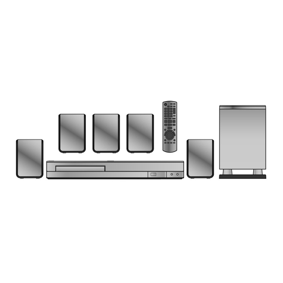
DVD Home Theater Sound System
Model No.
Product Color: (K)...Black Type
PAGE
to Electrostatic Sensitive (ES) Devices---------------6
2.2. Precaution of Laser Diode -------------------------------7
2.4. Handling Precautions for Traverse Unit --------------9
3 Service Navigation --------------------------------------------- 11
© Panasonic Corporation 2011. All rights reserved.
Unauthorized copying and distribution is a violation
of law.
SA-XH50P
SA-XH50PC
PSG1104002CE
A6
PAGE
Advertisement
Table of Contents
Troubleshooting

Related Manuals for Panasonic SA-XH50P


Summary of Contents for Panasonic SA-XH50P
-
Page 1: Table Of Contents
2.3. Service caution based on Legal restrictions --------8 1.4. Safety Parts Information --------------------------------- 5 2.4. Handling Precautions for Traverse Unit --------------9 2 Warning -------------------------------------------------------------- 6 3 Service Navigation --------------------------------------------- 11 © Panasonic Corporation 2011. All rights reserved. Unauthorized copying and distribution is a violation of law. - Page 2 3.1. Service Information -------------------------------------- 11 12.2. Backend P.C.B. (2/3)------------------------------------ 73 4 Specifications ---------------------------------------------------- 12 12.3. Backend P.C.B. (3/3)------------------------------------ 74 4.1. Others (Licences) ---------------------------------------- 13 12.4. Main P.C.B. (1/3)----------------------------------------- 75 5 Location of Controls and Components------------------ 14 12.5. Main P.C.B. (2/3)----------------------------------------- 76 5.1.
-
Page 3: Safety Precautions
1 Safety Precautions 1.1. GENERAL GUIDELINES 1. When servicing, observe the original lead dress. If a short circuit is found, replace all parts which have been overheated or damaged by the short circuit. 2. After servicing, see to it that all the protective devices such as insulation barriers, insulation papers shields are properly installed. -
Page 4: Before Repair And Adjustment
1.2. Before Repair and Adjustment Disconnect AC power to discharge unit AC Capacitors as such (C5702, C5703, C5704, C5705, C5706) through a 10 Ω, 10 W resis- tor to ground. Caution: DO NOT SHORT-CIRCUIT DIRECTLY (with a screwdriver blade, for instance), as this may destroy solid state devices. After repairs are completed, restore power gradually using a variac, to avoid overcurrent. -
Page 5: Protection Circuitry
1.3. Protection Circuitry The protection circuitry may have operated if either of the following conditions are noticed: • No sound is heard when the power is turned on. • Sound stops during a performance. The function of this circuitry is to prevent circuitry damage if, for example, the positive and negative speaker connection wires are “shorted”, or if speaker systems with an impedance less than the indicated rated impedance of the amplifier are used. -
Page 6: Warning
2 Warning 2.1. Prevention of Electrostatic Discharge (ESD) to Electrostatic Sensitive (ES) Devices Some semiconductor (solid state) devices can be damaged easily by static electricity. Such components commonly are called Elec- trostatically Sensitive (ES) Devices. Examples of typical ES devices are integrated circuits and some field-effect transistors and semiconductor “chip”... -
Page 7: Precaution Of Laser Diode
2.2. Precaution of Laser Diode Caution: This product utilizes a laser diode with the unit turned “on”, invisible laser radiation is emitted from the pickup lens. Wavelength: 655 nm (DVD)/790 nm (CD) Maximum output radiation power from pickup: 100 µW/VDE Laser radiation from the pickup unit is safety level, but be sure the followings: 1. -
Page 8: Service Caution Based On Legal Restrictions
2.3. Service caution based on Legal restrictions 2.3.1. General description about Lead Free Solder (PbF) The lead free solder has been used in the mounting process of all electrical components on the printed circuit boards used for this equipment in considering the globally environmental conservation. The normal solder is the alloy of tin (Sn) and lead (Pb). -
Page 9: Handling Precautions For Traverse Unit
2.4. Handling Precautions for Traverse Unit The laser diode in the optical pickup unit may break down due to static electricity of clothes or human body. Special care must be taken avoid caution to electrostatic breakdown when servicing and handling the laser diode in the traverse unit. Cautions to Be Taken in Handling the Optical Pickup Unit 2.4.1. - Page 10 2.4.2.2. Human body grounding 1. Use the anti-static wrist strap to discharge the static electricity form your body. Figure 2...
-
Page 11: Service Navigation
3 Service Navigation 3.1. Service Information This service manual contains technical information which will allow service personnel’s to understand and service this model. Please place orders using the parts list and not the drawing reference numbers. If the circuit is changed or modified, this information will be followed by supplement service manual to be filed with original service manual. -
Page 12: Specifications
4 Specifications (7) CD, CD-R/RW (CD-DA, Video CD, SVCD *2, 4 , MP3 *3,4 JPEG Main unit SA-XH50P/PC Conforming to IEC62107 GENERAL Power supply: AC 120 V, 60 Hz MPEG-1 Layer 3, MPEG-2 Layer 3, MPEG-2.5 Layer 3 Power consumption: Main Unit 47 W Exif Ver 2.0 JPEG Baseline files... -
Page 13: Others (Licences)
4.1. Others (Licences) -
Page 14: Location Of Controls And Components
5 Location of Controls and Components 5.1. Remote Control and Main Unit Key Button Operations... -
Page 15: Main Unit Key Button Operations
5.2. Main Unit Key Button Operations MUSIC PORT 5.3. Power-Saving Features POWER-SAVING FEATURES The main unit is designed to conserve its power consumption and save energy. Auto power-down function The main unit will automatically switch to standby mode after 30 minutes of inactivity. e.g. -
Page 16: Speaker Connection
5.4. Speaker Connection... -
Page 17: Linked Operations With The Tv (Viera Link "Hdavi Control™")
5.5. Linked Operations with the TV (VIERA LINK “HDAVI Control™”) -
Page 19: Connection With An Arc Compatible Tv
5.6. Connection with an ARC compatible TV... -
Page 20: Disc Information
5.7. Disc Information 5.7.1. Discs that can be played Commercial discs Region number DVD-V Type of media/ Remarks Indicated as Logo The player plays DVD-Video marked with labels containing the region DVD-Video High quality movie and DVD-V number “1” or “ALL”. music discs e.g. - Page 21 5.7.2. File Extension Type Support (MP3/JPEG)
-
Page 22: Operating Instructions
6 Operating Instructions 6.1. Removing of disc during abnomality 6.1.1. Using main unit key buttons. 6.1.1.1. When the power can be turned off. 1. Turn off the power and press & hold [OPEN/CLOSE] button on main unit and [SKIP FWD] button on remote for 5 seconds 6.1.1.2. - Page 23 3. Gently pull out the tray. 4. Remove disc...
-
Page 24: Self-Diagnostic And Special Mode Setting
7 Self-Diagnostic and Special Mode Setting 7.1. Cold-Start Here is the procedure to carry out cold-start for initialize to shipping mode. 1. Unplug AC power cord 2. Press & hold [POWER] button 3. Plug AC power cord while [POWER] button being pressed FL Display will show “_ _ _ _ _ _ _ _”... - Page 25 7.2.1. Service Mode Table 1 (For DVD) Item Key Operation FL Display Mode Name Description Front Key Error code Error code check In STOP (no disc) mode, check The latest error code stored in the press [OPEN/CLOSE] EEPROM IC is displayed. button on the main unit, and [0] button on the remote control unit.
- Page 26 7.2.2. Service Mode Table 2 (For DVD) Item Key Operation FL Display Mode Name Description Front Key DVD laser DVD laser drive current measurement. In STOP (no disc) mode, drive current For DVD laser drive current, refer to press [OPEN/CLOSE] measurement Troubleshooting Guide (Section 8.2) button on the main unit,...
- Page 27 7.2.3. Service Mode Table 3 (For DVD) Item Key Operation FL Display Mode Name Description Front Key Micro-processor Micro-processor firmware version In STOP (no disc) (Display 1) firmware version display & EEPROM checksum display. mode, press display & EEPROM checksum is only available [OPEN/CLOSE] button on EEPROM due to existence of EEPROM IC.
- Page 28 7.2.4. Service Mode Table 4 (For DVD) Item Key Operation FL Display Mode Name Description Front Key DVD firmware version is displayed on In STOP (no disc) firmware the FL Display. mode, press version display The firmware version can be updated [OPEN/CLOSE] button on using recovery disc.
- Page 29 Product TV Broadcasting Series Country Region Selected Region Display System OSD Language Code Code TV System (Default) Default USA, Canada, English (NA), Spanish (NA), P, PC, PX, NTSC AUTO2 (*A) English US Militry Canadian, French (blank) Japan NTSC AUTO2 (*A) Japanese Japanese, English English (EU), French, German,...
-
Page 30: Self-Diagnostic Mode
7.3. Self-Diagnostic Mode Item Key Operation FL Display Mode Name Description Front Key Press & hold Self-Diagnostic To enter into self-diagnostic checking [OPEN/CLOSE] on main Mode unit, follow by [4] then [9] on remote control. (When no disc in mechanism) Error code will display Error code System will perform a check on... -
Page 31: Self Diagnostic Function-Error Code
7.4. Self Diagnostic Function-Error Code 7.4.1. Mechanism Error Code Table (BRS1D) Error Diagnosis Contents Description of error Automatic FL Display Remarks Code H01 Tray loading error The tray opening and closing is abnormal. Press [OPEN/CLOSE] on main unit for next error. CLOSE and OPEN of the tray cannot be carried out properly. - Page 32 7.4.3. Power Supply & Digital Amplifier Error Code Table Error Diagnosis Contents Description of error Automatic FL Display Remarks Code F61 The abnormalities In normal operation, when DCDET2 goes ] on Press [OPEN/CLOSE in the D-Amp related to "L" (Low) (Not during POWER OFF main unit for next error.
-
Page 33: Sales Demonstration Lock Function
7.5. Sales Demonstration Lock Function This function prevents discs from being lost when the unit is used for sales demonstrations by disabling the disc eject function. “LOCKED” is displayed on the unit, and ordinary operation is disabled. 7.5.1. Setting • Prohibiting removal of disc 1. -
Page 34: Firmware Version-Up Information
7.6. Firmware Version-Up Information 7.6.1. Process Flow (1/2) Item FL/ GUI Display Remarks Process Description Collect ROM Step 1 Display 1: User can put both files Files Unzip the filmware update file. into the same root (Copy files into Step 2 directory. - Page 35 7.6.2. Process Flow (2/2) Item FL/ GUI Display Remarks Process Description GUI Display 1.3: To initialize, press and hold Update Completed main unit [STOP] then If firmware software update press remote control key completes successfully: [>10]. GUI Display 1.3: Firmware update is completed, please open the tray and remove the disc FL Display (Main Unit) will...
-
Page 36: Troubleshooting Guide
8 Troubleshooting Guide 8.1. Troubleshooting Guide for F61 and/or F76 This section illustrates the checking procedures when upon detecting the error of “F61” and/or “F76” after power up of the unit. It is for purpose of troubleshooting and checking in SMPS P.C.B.. Symptom(s) Possible Fault(s) Checking items... - Page 37 8.1.1. SMPS P.C.B. AC Inlet Jack : P5701 Regulator IC : Thermal Diaod : Photocoupler : IC2900 D5706 PC701 Fuse : F1 FFC Conector : H2016 H2016 Transformer : T5701 Fig. 1. SMPS P.C.B.
- Page 38 8.1.2. Main P.C.B. DC/DC CONVERTER IC: IC106 Inductors : L125 Inductors : L421 Resistor:R100 Transistor:Q107 Conector:CN100 Chip Jumper:K304 Fig. 2. Main P.C.B.
-
Page 39: Dvd/Cd Laser Diode Current
8.2. DVD/CD Laser Diode current measurement. This section will illustrate proceddures of measuring& deriving DVD/CD Laser Diode Current. Item Description Checking Item/ Formula Remarks 1. Measurement the voltage (V ) on the testpoints CL8530(+) & CL8531(-). Refer to 8.2.1. CD Laser Diode Current Measurement Backend P.C.B. - Page 40 8.2.1. Backend P.C.B (Side A of Backend P.C.B.) R8556 R8566 (Side B of Backend P.C.B.) CL8530, CL8531, CL8532 Fig. 3. Backend P.C.B.
-
Page 41: Basic Troubleshooting Guide For Traverse Unit (Backend P.c.b.)
8.3. Basic Troubleshooting Guide for Traverse Unit (Backend P.C.B.) Problems Checking Points Checking components 1) Distorted picture or a) Check SDRAM address, data IC8051 abnormal sound is head bus, CLK and other control signals during the initialization waveform b) Check video signals (CVBS) LB8317, R8325 (CVBS) c) Check audio DAC circuitry LB8422 till LB8428... -
Page 42: Basic Troubleshooting Guide For Hdmi Av Output
8.4. Basic Troubleshooting Guide for HDMI AV output Problems Checking Points Checking components 1) TV does not have any 1) Check setting of the set in * This year HDMI always ON. display. Set FL display Setup Menu whether the HDMI No need check Setup Menu. -
Page 43: Service Fixture & Tools
9 Service Fixture & Tools 9.1. Service Tools and Equipment Prepare service tools before process service position. Ref. No Service Tools Remarks SFT1 Main P.C.B. (CN201) - Backend P.C.B. (FP8101) RFKZXH150PK2 (50P FFC) -
Page 44: Disassembly And Assembly Instructions
10 Disassembly and Assembly Instructions Caution Note: • This section describes the disassembly and/or assembly procedures for all major printed circuit boards & main compo- nents for the unit. (You may refer to the section of “Main components and P.C.B Locations” as described in the service manual) •... -
Page 45: Disassembly Flow Chart
10.1. Disassembly Flow Chart 10.3. Top Cabinet 10.5. Front Panel 10.10. Main P.C.B. 10.4. Rear Panel Assembly 10.11. Digital Amplifier 10.8. DVD Mechanism 10.6. Panel P.C.B. Unit (BRS1D) IC (IC403/IC404/IC405) 10.7. Power Button 10.9. Traverse Unit 10.12. SMPS P.C.B. P.C.B. 10.13. -
Page 46: Main Components And P.c.b. Locations
10.2. Main Components and P.C.B. Locations... -
Page 47: Disassembly Of Top Cabinet
10.3. Disassembly of Top Cabinet Step 6 Remove Top Cabinet as arrow shown. Step 1 Remove 2 screws. Step 2 Remove 3 screws. Caution: Replace the Top Cabinet Insulator sheet if broken. Ensure it is pasted properly on Top Cabinet as diagram shown. -
Page 48: Disassembly Of Rear Panel
10.4. Disassembly of Rear Panel 10.5. Disassembly of Front Panel Assembly • Refer to “Disassembly of Top Cabinet” • Refer to “Disassembly of Top Cabinet”. Step 1 Remove 6 screws. Step 2 Remove 1 screw. Step 1 Detach 17P FFC at the connector (CN203) on Main/D- Amp P.C.B.. -
Page 49: Disassembly Of Panel P.c.b
Caution: Do not exert strong force when releasing the tabs. 10.6. Disassembly of Panel P.C.B. • Refer to “Disassembly of Top Cabinet”. • Refer to “Disassembly of Front Panel Assembly”. Step 1 Remove 5 screws. Step 2 Remove 1 screw. Step 3 Lift up Panel P.C.B.. - Page 50 Caution : Keep the Ground Spring in safe place, place it Caution: During assembling, ensure that 17P FFC is back during assembling. dressed as diagram shown. Step 6 Desolder 3P Wire at the cable holder (H902) on Panel P.C.B.. Step 7 Remove Panel P.C.B..
-
Page 51: Disassembly Of Power Button P.c.b
10.7. Disassembly of Power Button Step 3 Release 3P wire from wall & ribs of Front Panel. Caution: During assembling, ensure that 3P wire is prop- P.C.B. erly dressed in between wall & ribs of Front Panel as dia- gram shown. •... -
Page 52: Disassembly Of Dvd Mechanism Unit (Brs1D)
10.8. Disassembly of DVD Mecha- Step 4 Upset the Unit. Step 5 Release 2 catches. nism Unit (BRS1D) Caution: During assembling, ensure that Tray Ornament is inserted & fully catched onto Tray. • Refer to “Disassembly of Top Cabinet” Step 1 Insert Paper Clip into the hole on the Bottom Chassis Assembly. - Page 53 Caution: During assembling, ensure that Tray Ornament’s Step 8 Detach 24P FFC at the connector (FP8531) on Backend guide rib is properly inserted onto Tray. P.C.B.. Step 9 Detach 6P FFC at the connector (FP8251) on Backend P.C.B.. Step 10 Detach 5P FFC at the connector (FP8252) on Backend P.C.B..
-
Page 54: Replacement Of Traverse Unit
Step 12 Slightly lift up DVD Mechanism Unit (BRS1D). 10.9. Replacement of Traverse unit Step 13 Remove the DVD Mechanism Unit (BRS1D) in the • Refer to “Disassembly of DVD Mechanism Unit direction of arrow. (BRS1D)”. Caution: Refer to 2.4 “Handling Precaution for Traverse Unit”... - Page 55 Step 2 : Slide the tray out fully. Step 3 : Release the catches & remove the tray. Step 5 : Release the 24P FFC from the slot. Step 4 : Release the guide as shown & slide the Traverse Slide Plate to the end.
- Page 56 Step 6 : Lift the Traverse Unit by approximately 45°. Step 7 : Slide out the traverse unit as arrow shown. Caution : Avoid touching the surface of the traverse unit. 10.9.2. Assembly of Traverse Unit Step 1 : Release the guide as shown & slide the Traverse Slide Plate to the end.
- Page 57 Step 2 : Slot the Traverse unit at approximately 45° into the Step 3 : Ensure the Traverse Unit seated properly onto the mecha chassis as arrow shown. Groove. Step 4 : Slide Traverse Slide Plate to lock the Traverse Unit as shown.
- Page 58 Step 5 : Slot the FFC onto the slot. Caution : Ensure that the FFC are properly inserted into the slots as shown. Step 6 Slide the Traverse Slide Plate unit it stop at the Guide. Step 8 Ensure the Guides are align with the groove when slid- ing the tray in.
-
Page 59: Disassembly Of Main P.c.b
Step 9 Slide the tray in fully. 10.10. Disassembly of Main P.C.B. • Refer to “Disassembly of Top Cabinet”. Step 1 Remove 5 screws. Step 2 Remove 1 screw. Step 3 Position Rear Panel according to diagram shown. Step 4 Detach 50P FFC at the connector (CN201) on Main P.C.B.. - Page 60 Step 8 Remove Main P.C.B.. Caution: During assembling, ensure that Main P.C.B. is properly located & fully seated onto Bottom Chassis. Step 7 Remove 2 screws on Main P.C.B..
-
Page 61: Replacement Of Digital Amplifier Ic (Ic403/ Ic404/Ic405)
Caution: Replace the D-Amp Heat Radiator if torn. Ensure 10.11. Replacement of Digital Ampli- that D-Amp heat radiator is properly aligned & fully pasted fier IC (IC403/IC404/IC405) onto Bottom Chassis • Refer to “Disassembly of Top Cabinet”. • Refer to “Disassembly of Main P.C.B.”. 10.11.1. - Page 62 Step 3 Lift up Main P.C.B. as arrow shown. 10.11.2. Assembly of Digital Amplifier IC Caution: Keep the Heatsink Spacer in safe place. Avoid (IC403/IC404/IC405) denting it, place it back during assembling. Step 1 Fix the Digital Amplifier IC (IC403) onto the Main P.C.B.. Step 2 Solder pins of Digital Amplifier IC (IC403).
-
Page 63: Disassembly Of Smps P.c.b
Step 4 Upset the Main P.C.B.. 10.12. Disassembly of SMPS P.C.B. Step 5 Fix Heatsink spacers onto D-Amp Heatsink. • Refer to “Disassembly of Top Cabinet”. Step 6 Fix 3 screws. Note: For assembling of Digital Amplifier IC (IC404) & (IC405), Step 1 Remove 5 screws. - Page 64 Step 4 Remove 4 screws. Caution: Replace the Bottom PC Sheet if broken Ensure that it is pasted on the Bottom Chassis properly. Step 5 Lift up to remove SMPS P.C.B.. Caution: Handle the SMPS P.C.B. with care. Avoid touching the heatsink due to its prolong use.
-
Page 65: Replacement Of Current Limiting Switch (Q5701)
10.13. Replacement of Current Limit- 10.13.2. Assembly Current Limiting Switch (Q5701) ing Switch (Q5701) Step 1 Apply grease to the Heatsink Ext A. • Refer to “Disassembly of Top Cabinet”. Step 2 Fix the Current Limiting Switch (Q5701) to the SMPS •... -
Page 66: Replacement Of Diode (D5706)
10.14. Replacement of Diode (D5706) 10.14.2. Assembly of Diode (D5706) Step 1 Apply grease to the Heatsink Ext B. • Refer to “Disassembly of SMPS P.C.B.”. Step 2 Fix the Diode (D5706) to the SMPS P.C.B.. • Refer to “Disassembly of Top Cabinet. Caution: Ensure pins of the Diode (D5706) are properly 10.14.1. -
Page 67: Disassembly Of Backend P.c.b
10.15. Disassembly of Backend P.C.B. • Refer to “Disassembly of Top Cabinet”. Step 1 Remove 1 screw. Step 2 Remove 1 screw. Step 3 Release the tab of the side of the Rear Panel in the direction of arrow. Step 10 Lift up the Backend P.C.B.. Step 4 Detach 24P FFC at the connector (FP8531) on Backend P.C.B.. - Page 68 Step 12 Remove Backend P.C.B. Shield Plat Unit. Caution : During assembling, replace the B/E Heat Radia- tor if torn. Ensure that B/E Heat Radiator is properly located & fully pasted within embossing on Backend P.C.B Shield Plate Caution : During assembling, ensure that Backend P.C.B. Shield Plate Unit is properly inserted and fully seated onto Backend P.C.B..
-
Page 69: Service Position
11 Service Position 11.2. Checking & Repairing Main P.C.B. (Side A) Note: For description of the disassembly procedures, see the Section 10. Step 1 Remove Top Cabinet. Step 2 Remove Rear Panel. 11.1. Checking & Repairing Main Step 3 Remove 2 screws. P.C.B. -
Page 70: Checking & Repairing Of Smps P.c.b
11.3. Checking & Repairing of SMPS 11.5. Checking & Repairing of DVD P.C.B. Module P.C.B. Step 1 Remove Top Cabinet. 11.5.1. Checking & Repairing of Backend Step 2 Remove SMPS P.C.B.. P.C.B. (Side B) Step 3 Position SMPS P.C.B. on the insulated material. Step 4 Connect 12P cable at the connector (CN100) on Main Step 1 Remove Top Cabinet. - Page 71 11.5.2. Checking & Repairing of Backend P.C.B. (Side A) Step 1 Remove Top Cabinet. Step 2 Remove Backend P.C.B.. Step 3 Connect 24P FFC at the connector (FP8531) on Back- end P.C.B.. Step 4 Connect 6P FFC at the connector (FP8251) on Backend P.C.B..
-
Page 72: Voltage & Waveform Chart
CD PLAY STANDBY REF NO. IC8001 MODE CD PLAY STANDBY IC8001 REF NO. MODE CD PLAY STANDBY IC8001 REF NO. MODE CD PLAY STANDBY IC8001 REF NO. MODE CD PLAY STANDBY IC8001 REF NO. MODE CD PLAY STANDBY SA-XH50P/PC BACKEND P.C.B. -
Page 73: Backend P.c.b. (2/3)
CD PLAY STANDBY IC8251 REF NO. MODE CD PLAY STANDBY IC8251 REF NO. MODE CD PLAY STANDBY IC8606 REF NO. MODE CD PLAY STANDBY IC8651 REF NO. MODE CD PLAY STANDBY IC9006 REF NO. MODE CD PLAY STANDBY SA-XH50P/PC BACKEND P.C.B. -
Page 74: Backend P.c.b. (3/3)
12.3. Backend P.C.B. (3/3) Q3901 Q3902 Q3903 Q3904 Q8552 REF NO. MODE CD PLAY -1.1 STANDBY -1.1 REF NO. Q8562 Q8565 MODE CD PLAY STANDBY SA-XH50P/PC BACKEND P.C.B. -
Page 75: Main P.c.b. (1/3)
REF NO. IC200 MODE CD PLAY STANDBY IC200 REF NO. MODE CD PLAY STANDBY IC201 REF NO. MODE CD PLAY STANDBY IC202 REF NO. MODE CD PLAY STANDBY REF NO. IC300 MODE CD PLAY -5.0 STANDBY -5.0 SA-XH50P/PC MAIN P.C.B. -
Page 76: Main P.c.b. (2/3)
REF NO. IC404 MODE CD PLAY STANDBY IC404 REF NO. MODE CD PLAY 10.1 20.3 20.3 10.1 10.2 20.3 10.2 10.2 20.3 10.2 10.2 20.3 STANDBY 10.1 20.3 20.3 10.1 10.2 20.3 10.2 10.2 20.3 10.2 10.2 20.3 SA-XH50P/PC MAIN P.C.B. -
Page 77: Main P.c.b. (3/3)
-5.6 -25.4 -0.4 REF NO. Q106 Q107 Q114 Q116 Q200 MODE CD PLAY 12.1 10.0 20.6 STANDBY 12.1 10.0 20.6 Q201 Q300 Q301 Q500 Q501 REF NO. MODE CD PLAY 10.1 10.3 10.3 STANDBY 10.1 10.3 10.3 SA-XH50P/PC MAIN P.C.B. -
Page 78: Panel P.c.b
REF NO. MODE POWER ON -22.9 -22.8 STANDBY -22.9 -22.8 REF NO. Q900 Q901 MODE POWER ON STANDBY SA-XH50P/PC PANEL P.C.B. 12.8. SMPS P.C.B. REF NO. IC2900 MODE POWER ON 20.1 12.1 STANDBY 20.1 12.1 IC5701 REF NO. MODE POWER ON... -
Page 79: Waveform Table (1/2)
12.9. Waveform Table (1/2) 1.5Vp-p(50nsec/div) 2Vp-p(50nsec/div) 0.4Vp-p(200usec/div) 0.06Vp-p(2usec/div) 1.25Vp-p(2usec/div) 0.15Vp-p(2usec/div) 0.05Vp-p(2usec/div) 2Vp-p(20nsec/div) 1Vp-p(20nsec/div) 3.2Vp-p(500nsec/div) 3.6Vp-p(500nsec/div) 6Vp-p(1usec/div) 6Vp-p(1usec/div) 6Vp-p(500nsec/div) 6Vp-p(1usec/div) 32Vp-p(1usec/div) 6Vp-p(1usec/div) 32Vp-p(1usec/div) 6Vp-p(1usec/div) 32Vp-p(1usec/div) -
Page 80: Waveform Table (2/2)
12.10. Waveform Table (2/2) 4.8Vp-p(2usec/div) 1.25Vp-p(50usec/div) 5Vp-p(1usec/div) 0.4Vp-p(200usec/div) 2Vp-p(20nsec/div) -
Page 81: Illustration Of Ics, Transistor And Diode
13 Illustration of ICs, Transistor and Diode RFKWMXH50EB VUEALLPT040 (20P) C0DBAYY00927 (8P) RFKWMH0933E0 (48P) C1AB00003216 (64P) (100P) C0DBGYY00887 (4P) C0FBAK000026 (16P) C0HBB0000057 (44P) C0DBZYY00448 (8P) C0JBAR000540 (16P) C1AB00003217 (44P) C0ABBB000230 (8P) C3EBFC000042 (8P) C0JBAR000433 (8P) No.1 C0DBZYY00018 (8P) No.1 C3ABPG000163 (54P) No.1 No.1 C0DBAYH00005... -
Page 83: Overall Simplified Block Diagram
14 Overall Simplified Block Diagram MAIN BLOCK TUNER DIGITAL AMP BLOCK (TI Solution) HDMI D-IN Composite FRONT L FRONT R MCLK,BCLK,SRCK SURR L CP IC Video HDMI Buffer SURR R MCLK,BCLK,SRCK FLASH DVD Decoder SELECTOR CENTER SDRAM +5.3V Motor SUBWOOFER UART Driver +5.3V... -
Page 84: Block Diagram
FROM/TO SYSTEM CONTROL LOAD SWITCH FP8252 FP8101 CN201 CLOSE SW CLOSE SW CLOSE SW CLOSE SW FP8252 FP8101 CN201 OPEN SW OPEN SW OPEN SW OPEN SW NOTE: “ * ” REF IS FOR INDICATION ONLY SA-XH50P/PC BACKEND BLOCK DIAGRAM... -
Page 85: Ic Terminal Chart
MDQ 4 MDQ 5 MDQ 6 MDQ 7 MDQ 8 MDQ 9 DQ10 MDQ 10 DQ10 DQ11 MDQ 11 DQ11 DQ12 MDQ 12 DQ12 DQ13 MDQ 13 DQ13 DQ14 MDQ 14 DQ14 DQ15 MDQ 15 DQ15 SA-XH50P/PC IC TERMINAL CHART... -
Page 86: System Control
VBUS EN ECO CNTRL ECO CNTRL ECO CNTRL PCONT PCONT PCONT FROM/TO SYNC SYNC SYNC POWER SUPPLY DC DET1 DC DET1 DC DET1 DC DET2 DC DET2 DC DET2 USB OC USB OC USB OC SA-XH50P/PC SYSTEM CONTROL BLOCK DIAGRAM... -
Page 87: Audio & Video
TUN SDIO TUN SDIO TUN SDIO SDIO 8 JK300 PANEL P.C.B. JK902 IC301 C0ABBB000230 OP-AMP MPORT RCH CN901 CN203 MPORT RCH MPORT RCH MUSIC PORT MPORT LCH CN901 CN203 MPORT LCH MPORT LCH SA-XH50P/PC AUDIO & VIDEO (1/2) BLOCK DIAGRAM... - Page 88 VALID 7 RST AB OUT D SUBWOOFER JK401 17 RST CD OUT C 2 OTW BST C DC DETECT DC DET2 DC DET2 CIRCUIT Q114,Q116 FROM DC DET2 Q500,Q501 DC DET2 POWER SUPPLY SA-XH50P/PC AUDIO & VIDEO (2/2) BLOCK DIAGRAM...
-
Page 89: Power Supply
ISENSE 4 Q5841 Q5701 DC DET1 CURRENT LIMITING DC DETECT SWITCH P5701 D5701 AC INLET L5701 L5702 DZ5701 TH5702 COLD TO POWER SUPPLY BLOCK (2/2) NOTE: “ * ” REF IS FOR INDICATION ONLY SA-XH50P/PC POWER SUPPLY (1/2) BLOCK DIAGRAM... - Page 90 7 EN FB 5 Q101 PCONT PCONT POWER CONTROL IC107 C0DBZYY00018 +3.3V REGULATOR TO POWER SUPPLY PW 3.3V D, PW 3.3V DAP 3.3V CONT BLOCK (1/2) NOTE: “ * ” REF IS FOR INDICATION ONLY SA-XH50P/PC POWER SUPPLY (2/2) BLOCK DIAGRAM...
-
Page 91: Wiring Connection Diagram
P5701 SENSOR SMPS P.C.B. AC IN (SOLDER SIDE) Z901 120V 60Hz PANEL P.C.B. (SOLDER SIDE) H902 T2900 JK902 (SWITCHING TRANSFORMER) CN901 T5701 H2016* (MAIN TRANSFORMER) MUSIC PORT NOTE: " * " REF IS FOR INDICATION ONLY. SA-XH50P/PC WIRING CONNECTION DIAGRAM... -
Page 93: Schematic Diagram
17 Schematic Diagram • Voltage and signal line : +B signal line : -B signal line 17.1. Schematic Diagram Notes : Audio output signal line • This schematic diagram may be modified at any time : Video output signal line with the development of new technology. -
Page 95: Backend Circuit
R8322 JK8301 VGND VGND L2802 R8326 LB8304 LB8317 R8325 C2823 VIDEO OUT J0JBC0000015 100P VIDEO (YEL) JK8001 TO BACKEND CIRCUIT (2/6) C8030 DIGITAL AUDIO IN 6.3V33 OPT-IN (OPTICAL) R8025 OPT_IN L8001 G1C100M00049 D+3R3V TO BACKEND CIRCUIT (4/6) SA-XH50P/PC BACKEND CIRCUIT... - Page 96 K3901 C0JBAR000433 FRAME LB3907 MULTIPLEXER J0JCC0000308 G3 G4 R3955 K3902 R3958 K3903 LB3909 J0JHC0000045 C3958 R3908 C3972 R3959 SPDIF_SW SELECT C3970 C3967 R3956 R3900 100K IC3953 GPIO34 C0JBAB000986 TO BACKEND INVERTER CIRCUIT (1/6) TO BACKEND CIRCUIT (5/6) SA-XH50P/PC BACKEND CIRCUIT...
- Page 97 L8552 R8621 X8621 G1C100M00049 R8622 220K H0J270500131 C8621 L8302 G1C100M00049 K8301 R8311 1000P C8006 100P C8029 1000P LB3902 J0JHC0000045 C8028 0.01 VDDP_HDMI LB3901 J0JHC0000045 VDDDAC LB8301 J0JHC0000045 C3902 C3901 C8301 6.3V100 6.3V100 6.3V100 TO BACKEND CIRCUIT (6/6) SA-XH50P/PC BACKEND CIRCUIT...
- Page 98 DUPTDO FOR FIRMWARE +3.3V REGULATOR DUPRDO +1.8V REGULATOR DUPRDO DOWNLOAD DGND DGND 3.3V 1.8V C8101 C8113 FP8002 VDD_3R3V DUPTDI DUPTDI FOR FIRMWARE CL8101 DUPRDI DUPRDI R8101 DEBUG 1.47K DGND DOWNLOAD DOWNLOAD C8112 C8111 R8102 C8114 470P DGND SA-XH50P/PC BACKEND CIRCUIT...
- Page 99 RFIN_P D1H456020001 R8542 RF_A RX8532 RF_B D1H456020001 RF_F R8537 PD GND TO OPTICAL PICKUP UNIT VC(REF) (DVD MECHANISM UNIT BRS1D) LB8531 C8533 RF_E R8538 DVD_MD R8531 VR-CD LB8561 VR-DVD J0JDC0000102 CD-LD LB8551 J0JDC0000102 DVD-LD R8532 GND-LD CD_MD SA-XH50P/PC BACKEND CIRCUIT...
- Page 100 FL8104 F1J1E1040022 MGND ADGND TV_LIN ADGND R8051 TV_RIN FUNC_SW RGB_H UART_TX UART_TX LB8692 UART_RX C8051 UART_RX LB8691 OPEN_SW OPEN SW CLOSE_SW CLOSE_SW IC8051 VBUS_EN C8055 C3ABPG000163 USB_OC AMUTE SDRAM AMUTE ADGND MIC_IN MIC_IN VGND VGND iPod_VIDEO iPod_SW SA-XH50P/PC BACKEND CIRCUIT...
-
Page 101: Main Circuit
DGND K301 AGND CN202 PW_3.3VREF VREF BUSY BUSY LB200 CLOCK CLOCK SYS5VGND VOUT TO uP DOWNLOADER PW_SYS6V DGND RESET C214 LB201 C205 D201 CNVSS B0BC7R5A0263 IC202 CNVSS C0DBGYY00887 +3.3V REGULATOR RESET C219 0.01 TO MAIN CIRCUIT (5/8) SA-XH50P/PC MAIN CIRCUIT... - Page 102 CLOSE_SW R273 CLOSE_SW VBUS_EN R275 C453 VBUS_EN 0.01 R276 USB_OC USB_OC R268 AMUTE AMUTE R277 ADGND C451 MIC_IN C452 R278 K105 VGND L427 VGND J0JYC0000196 R435 iPod_VIDEO iPod_SW K158 TO MAIN CIRCUIT (3/8) TO MAIN CIRCUIT (6/8) SA-XH50P/PC MAIN CIRCUIT...
- Page 103 R212 R213 CLOSE_SW FLD_STB ECO_CNTRL CK_FLD R232 FLD_OUT SYNC RESET TUN_INT TUN_SCLK X201 H2D500400006 TUN_SDIO TUN_REST LED_CTRL R224 R294 R239 R254 R230 R223 R225 R226 10K...P TO MAIN 1.2K 1.2K 15K...PC CIRCUIT (2/8) TO MAIN CIRCUIT (7/8) SA-XH50P/PC MAIN CIRCUIT...
- Page 104 1000P PWM_D PVDD_D SP_FR+ C519 PVDD_D 25V330 C455 C171 L409 0.01 1000P G0A100H00018 R452 C510 0.033 BST_D R506 R453 GVDD_C GVDD_D SP_SL- C190 1000P C433 C432 C431 C514 C567 1000P K157 R454 CHASSIS TO MAIN CIRCUIT (8/8) SA-XH50P/PC MAIN CIRCUIT...
- Page 105 C322 330P 1000P C324 C321 C315 16V100 R319 C317 C316 R317 +VCC IC301 Q301 B1GBCFJJ0051 C0ABBB000230 R315 SWITCH OP-AMP R312 R313 -VCC R318 R316 C319 C327 C326 C325 330P 1000P Q300 B1GBCFJJ0051 SWITCH MPORT-RCH R323 R324 8.2K SA-XH50P/PC MAIN CIRCUIT...
- Page 106 CK_FLD R136 PW_SW5V_ADC FL_IC_CLK IN SCHEMATIC FLD_STB R137 FL_IC_STB DIAGRAM - 15 LB704 LED_CTRL R140 G1C100M00049 LED_CTRL KEY1 R138 KEY1 C708 KEY2 R133 KEY2 6.3V47 PW_FL+ R139 PW_FL- R141 PW_-VP R142 TO MAIN CIRCUIT (7/8) LB703 J0JCC0000317 SA-XH50P/PC MAIN CIRCUIT...
- Page 107 L125 B1ABCF000176 G0C330M00002 DC DETECT Q100 R152 C135 0.01 B1CHPD000003 C198 C142 R150 C138 C141 C143 C129 POWER SUPPLY 25V4.7 0.47 25V470 SYS5VGND K107 D116 K104 Q101 B0JCPG000005 PW_SW5V_D K106 B1GBCFJJ0051 POWER CONTROL PW_SW5V_ADC K102 R196 K101 SA-XH50P/PC MAIN CIRCUIT...
- Page 108 GND_D R460 5.6K RST_CD(L) OUT_D PWM_SR- SP_SR+ C574 C559 PWM_D PVDD_D C554 PVDD_D 25V330 L405 G0A100H00018 R461 C550 0.033 BST_D PW_+12V R462 GVDD_C GVDD_D C439 C438 C437 C551 C441 K303 16V33 PVDD_D R463 C802 C803 C512 HEATSINK SA-XH50P/PC MAIN CIRCUIT...
-
Page 109: Panel & Power Button Circuit
R929 B1GBCFJJ0051 L904 LED CONTROL R919 C918 J0JYC0000196 MRCH MUSIC PORT C919 MLCH L905 R920 J0JYC0000196 R921 L907 J0JBC0000019 R930 CHASSIS POWER BUTTON CIRCUIT : +B SIGNAL LINE H901 S902 POWER DGND KEY1 VREF_LED SA-XH50P/PC PANEL / POWER BUTTON CIRCUIT... -
Page 110: Smps Circuit
C5726 1000P 0.33 R5731 R5729 R5730 4.7K Q5863 IC5702 B1ABCF000176 R5863 R5865 SWITCH C0DBZMC00006 4.7K SHUNT REGULATOR TO SMPS R5817 CIRCUIT (2/2) C5864 R5866 C5870 1.2K 100K 0.01 NOTE: “ * ” REF IS FOR INDICATION ONLY SA-XH50P/PC SMPS CIRCUIT... - Page 111 CTRL D5704 B0JCME000035 C5719 0.22 OPTMR ZA5703* R5724 HEATSINK 180K C5720 C5715 0.01 IC5701 C0DBZYY00448 SWITCH-MODE POWER SUPPLY CONTROLLER TH5701 R5723 D4CC11040013 D5705 B0BC02700039 TO SMPS CIRCUIT (1/2) NOTE: “ * ” REF IS FOR INDICATION ONLY SA-XH50P/PC SMPS CIRCUIT...
-
Page 112: Printed Circuit Board
(DVD MECHANISM UNIT BRS1D)) D8251 C8024 R8255 R8256 IC8111 R8253 CL8101 R8254 D8101 L8251 C8252 D8102 L8252 R8259 FL8103 FL8101 R8260 FL8104 FP8252 (TO LOADING PCB (DVD MECHANISM UNIT FP8101 BRS1D)) 0680A 0680A 0680A 0680A (SIDE A) (SIDE B) SA-XH50P/PC BACKEND P.C.B. -
Page 113: Main P.c.b
C214 C189 C501 C502 C132 R142 R530 C187 R195 C191 R157 R156 C197 C522 C523 C192 Q100 D114 C186 Q101 C181 C182 C472 C183 C184 C473 C185 C486 R406 R407 C135 K109 C512 0729A 0729A (SIDE A) SA-XH50P/PC MAIN P.C.B. - Page 114 C166 30 32 SUBWOOFER R469 R442 L418 C412 C411 1-SW+ R411 IC106 C410 C415 R404 R444 R413 C479 L421 R443 X400 C425 R412 JK401 C505 C420 R445 C138 C413 L419 C441 C143 L125 0729A 0729A (SIDE B) SA-XH50P/PC MAIN P.C.B.
-
Page 115: Panel & Power Button P.c.b
W921 FL901 W930 R930 H902 W925 S906 S905 C931 R929 JK902 R912 (VOL+) (VOL-) R924 W929 R913 D901 13 15 W933 CN901 MUSIC SENSOR PORT POWER BUTTON P.C.B. (REPX0890C) H901 S902 (POWER) 0731AB 0731AB SA-XH50P/PC PANEL / POWER BUTTON P.C.B. -
Page 116: Smps P.c.b
Q2900 IC5701 R5702 T5701 C5705 W1039 (MAIN TRANSFORMER) W1033 H2016* R5704 R5703 0730A 0730A CAUTION RISK OF ELECTRIC SHOCK AC VOLTAGE LINE. PLEASE DO NOT TOUCH THIS P.C.B NOTE: " * " REF IS FOR INDICATION ONLY. SA-XH50P/PC SMPS P.C.B. -
Page 117: Terminal Function Of Ics
19 Terminal Function of ICs Pin No. Terminal Name I/O Function No Connection No Connection 19.1. IC200 (RFKWMXH50EB): No Connection +3.3V System Supply MICROPROCESSOR No Connection System Ground No Connection Pin No. Terminal Name I/O Function NRST O ADC Reset CLOSE_SW Close Switch for BRS1D No Connection... -
Page 118: Ic6001 (C0Hbb0000057): Ic Fl Display Driver
19.2. IC6001 (C0HBB0000057): IC FL Display Driver Terminal Name Function LED1 No Connection LED2 No Connection LED3 No Connection LED4 No Connection Oscillator Input DOUT No Connection Data Input Clock Input Serial Interface Strobe Key Data Input 1 (No Connec- tion) Key Data Input 2 (No Connec- tion) -
Page 119: Exploded View And Replacement Parts List
T2900 *HEATSINK CLAMPER Z901 EXT A H902 CN203 *H2016 CN202 CN901 *HEATSINK (PANEL P.C.B.) EXT B ZJ5701 JK902 FL901 H901 (POWER BUTTON P.C.B.) SA-XH50P/PC-K NOTE: " * " PART IS NOT SUPPLIED / REF IS FOR INDICATION ONLY. CABINET DRAWINGS... - Page 120 20.1.2. Packaging ACCESSORIES BAG AC CORD FM INDOOR ANTENNA VIDEO CABLE SA-XH50P/PC A1-1 SB-XH50P/PC F R O N T POLYFOAM (LEFT) POLYFOAM (RIGHT) SC-XH50P/PC-K PACKAGING DRAWINGS...
- Page 121 20.1.3. Mechanical Replacement Part List Safety Ref. Part No. Part Name & Qty Remarks Description Safety Ref. Part No. Part Name & Qty Remarks RMQ1742 HIMELON SHEET Description RMZX1022 HEATSINK SPACER RSC1018 MAIN HEAT RADIA- CABINET CHASSIS RSCX1059 BACKEND SHIELD PLATE REEX1249 (MAIN- RSCX1060...
- Page 122 Safety Ref. Part No. Part Name & Qty Remarks Description RQTX1326-P O/I BOOK (En) RQTX1327-C O/I BOOK (Cf) RSAX0002 INDOOR ANTENNA K2KA2BA00001 VIDEO CABLE...
-
Page 123: Electrical Replacement Parts List
20.2. Electrical Replacement Parts List Safety Ref. Part No. Part Name & Qty Remarks Description Safety Ref. Part No. Part Name & Qty Remarks IC8051 C3ABPG000163 Description IC8111 C0DBEHG00006 PRINTED CIRCUIT IC8112 C0DBZYY00018 BOARDS IC8251 C0GBY0000117 IC8606 C0EBE0000504 PCB1 REPX0888D MAIN P.C.B. - Page 124 Safety Ref. Part No. Part Name & Qty Remarks Safety Ref. Part No. Part Name & Qty Remarks Description Description L600 G1CR18JA0020 INDUCTOR D101 B0BC5R6A0266 DIODE L904 J0JYC0000196 INDUCTOR D110 B0ACCK000012 DIODE L905 J0JYC0000196 INDUCTOR D111 B0ACCK000012 DIODE L906 J0JBC0000019 INDUCTOR D112 B0BC7R5A0263...
- Page 125 Safety Ref. Part No. Part Name & Qty Remarks Safety Ref. Part No. Part Name & Qty Remarks Description Description X8621 H0J270500131 CRYSTAL OSCILLA- K8003 ERJ2GE0R00X 1/16W K8007 ERJ2GE0R00X 1/16W K8008 ERJ2GE0R00X 1/16W FL DISPLAY K8102 D0GBR00JA008 1/16W K8251 D0GBR00JA008 1/16W FL901 A2BB00000175...
- Page 126 Safety Ref. Part No. Part Name & Qty Remarks Safety Ref. Part No. Part Name & Qty Remarks Description Description R207 D0GB103JA008 1/16W R293 D0GBR00JA008 1/16W R208 D0GB103JA008 1/16W R294 D0GB473JA008 1/16W R209 D0GB103JA008 1/16W R295 D0GBR00JA008 1/16W R210 D0GB102JA008 1/16W R296 D0GBR00JA008...
- Page 127 Safety Ref. Part No. Part Name & Qty Remarks Safety Ref. Part No. Part Name & Qty Remarks Description Description R448 D0GB101JA008 1/16W R900 D0GB473JA008 1/16W R449 D0GB101JA008 1/16W R901 D0GB680JA008 1/16W R450 D0GB223JA008 1/16W R902 D0GB102JA008 1/16W R451 D0GB101JA008 1/16W R903 D0GB680JA008...
- Page 128 Safety Ref. Part No. Part Name & Qty Remarks Safety Ref. Part No. Part Name & Qty Remarks Description Description R5730 ERJ3RBD472V 4.7K 1/16W RX8011 D1H88204A043 RESISTOR NETWORK R5731 ERJ3RBD393V 1/16W RX8012 D1H88204A043 RESISTOR NETWORK R5735 D0HB102ZA002 1/16W RX8013 D1H88204A043 RESISTOR NETWORK R5817 ERJ3RBD122V...
- Page 129 Safety Ref. Part No. Part Name & Qty Remarks Safety Ref. Part No. Part Name & Qty Remarks Description Description C307 F1H1C105A118 C456 F1H1H103A219 0.01uF C308 F1H1H681A013 680pF C460 F1H1H104A013 0.1uF C309 F1H1H681A013 680pF C461 F1H1H104A013 0.1uF C312 F1H1C105A118 C462 F1H1H104A013 0.1uF C313...
- Page 130 Safety Ref. Part No. Part Name & Qty Remarks Safety Ref. Part No. Part Name & Qty Remarks Description Description C802 F1H1H104A013 0.1uF C8009 F1G1A1040006 0.1uF C803 F1H1H104A013 0.1uF C8010 F1G1A1040006 0.1uF C804 F1J1H4740002 0.47uF C8011 F2G0J221A031 220uF 6.3V C805 F1J1H4740002 0.47uF C8012...
- Page 131 Safety Ref. Part No. Part Name & Qty Remarks Description SFT1 RFKZXH150PK2 50P FFC (MAIN TO BACKEND) MMH1104...