Table of Contents
Advertisement
CDC-R504MP/X504MP
SERVICE MANUAL
Ver 1.0 2004. 01
• The tuner and CD sections have no adjustments.
AUDIO POWER SPECIFICATIONS (US MODEL)
POWER OUTPUT AND TOTAL HARMONIC DISTORTION
23.2 watts per channel minimum continuous average power into
4 ohms, 4 channels driven from 20 Hz to 20 kHz with no more
than 5% total harmonic distortion.
Tuner section
FM
Tuning range
US, Canadian Model:
87.5 – 107.9 MHz
AEP, UK Model:
87.5 – 108 MHz
Antenna terminal
External antenna connector
Intermediate frequency 10.7 MHz/450 kHz
Usable sensitivity
9 dBf
Selectivity
75 dB at 400 kHz
Signal-to-noise ratio
67 dB (stereo),
69 dB (mono)
Harmonic distortion at 1 kHz
0.5% (stereo),
0.3% (mono)
Separation
35 dB at 1 kHz
Frequency response
30 – 15,000 Hz
AM (US, Canadian Model)
Tuning range
530 – 1,710 kHz
Antenna terminal
External antenna connector
Intermediate frequency 10.7 MHz/450 kHz
Sensitivity
30 µV
MW/LW (AEP, UK Model)
Tuning range
MW: 531 – 1,602 kHz
LW: 153 – 279 kHz
Antenna terminal
External antenna connector
Intermediate frequency 10.7 MHz/450 kHz
Sensitivity
MW: 30 µV
LW: 40 µV
CD player section
Signal-to-noise ratio
120 dB
Frequency response
10 – 20,000 Hz
Wow and flutter
Below measurable limit
Sony Corporation
9-877-518-01
2004A04-1
e Vehicle Company
© 2004. 01
Published by Sony Engineering Corporation
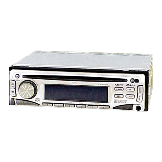
Photo: CDC-X504MP
Model Name Using Similar Mechanism
CD Drive Mechanism Type
Optical Pick-up Name
SPECIFICATIONS
Power amplifier section
Outputs
Speaker impedance
Maximum power output 52 W × 4 (at 4 ohms)
General
Outputs
Inputs
Tone controls
Power requirements
Dimensions
Mounting dimensions
Mass
Supplied accessories
Design and specifications are subject to change without
notice.
FM/AM COMPACT DISC PLAYER
FM/MW/LW COMPACT DISC PLAYER
US Model
Canadian Model
CDC-X504MP
AEP Model
UK Model
CDC-R504MP/X504MP
CDX-R3300/R3300T
MG-611MA-186//Q
KSS1000E
Speaker outputs
(sure seal connectors)
4 – 8 ohms
Audio outputs terminal (rear/sub switchable)
Power antenna relay control terminal
Power amplifier control terminal
Telephone ATT control terminal (AEP, UK Model)
Antenna input terminal
Low: ±10 dB at 60 Hz (HIP-HOP)
Mid: ±10 dB at 1 kHz (HIP-HOP)
High: ±10 dB at 10 kHz (HIP-HOP)
12 V DC car battery (negative ground)
Approx. 178 × 50 × 176 mm
(7
× 2 × 7 in.) (w/h/d)
1/8
Approx. 182 × 53 × 161 mm
(7
× 2
× 6
in.) (w/h/d)
1/4
1/8
3/8
Approx. 1.2 kg (2 lb. 10 oz.)
Parts for installation and connections (1 set)
Front panel case (1)
Card remote control RM-Z304
US, Canadian model
AEP, UK model
1
Advertisement
Table of Contents

Related Manuals for Aiwa CDC-R504MP


Summary of Contents for Aiwa CDC-R504MP
- Page 1 CDC-R504MP/X504MP SERVICE MANUAL US Model Canadian Model Ver 1.0 2004. 01 CDC-X504MP AEP Model UK Model CDC-R504MP/X504MP Photo: CDC-X504MP • The tuner and CD sections have no adjustments. Model Name Using Similar Mechanism CDX-R3300/R3300T CD Drive Mechanism Type MG-611MA-186//Q AUDIO POWER SPECIFICATIONS (US MODEL)
- Page 2 CDC-R504MP/X504MP SERVICE NOTES • US, Canadian model CAUTION Use of controls or adjustments or performance of procedures NOTES ON HANDLING THE OPTICAL PICK-UP BLOCK other than those specified herein may result in hazardous OR BASE UNIT radiation exposure. The laser diode in the optical pick-up block may suffer electrostatic breakdown because of the potential difference generated by the charged electrostatic load, etc.
- Page 3 CDC-R504MP/X504MP Notes on CD-Rs (recordable CDs)/CD-RWs (rewritable UNLEADED SOLDER CDs) Boards requiring use of unleaded solder are printed with the lead This unit can play the following discs: free mark (LF) indicating the solder contains no lead. (Caution: Some printed circuit boards may not come printed with the lead free mark due to their particular size.)
-
Page 4: Table Of Contents
CDC-R504MP/X504MP TABLE OF CONTENTS 1. GENERAL Location of Controls ..............5 Connections (US, Canadian Model) ........6 Connections (AEP, UK Model) ..........7 2. DISASSEMBLY 2-1. Sub Panel Assy ..............9 2-2. CD Mechanism Block ............9 2-3. Main Board ............... 10 2-4. -
Page 5: General
CDC-R504MP/X504MP SECTION 1 GENERAL This section is extracted from instruction manual. LOCATION OF CONTROLS... -
Page 6: Connections (Us, Canadian Model)
CDC-R504MP/X504MP CONNECTIONS (US, Canadian Model) -
Page 7: Connections (Aep, Uk Model)
CDC-R504MP/X504MP CONNECTIONS (AEP, UK Model) -
Page 8: Disassembly
CDC-R504MP/X504MP SECTION 2 DISASSEMBLY Note : This set can be disassemble according to the following sequence. 2-1. SUB PANEL ASSY (Page 9) 2-2. CD MECHANISM BLOCK (Page 9) 2-10. SERVO BOARD 2-3. MAIN BOARD 2-4. CHASSIS (T) SUB ASSY (Page 13) -
Page 9: Sub Panel Assy
CDC-R504MP/X504MP Note : Follow the disassembly procedure in the numerical order given. 2-1. SUB PANEL ASSY 3 two claws 2 two claws 1 two screws (+PTT 2.6 x 6) 4 sub panel assy 2-2. CD MECHANISM BLOCK 7 bracket (CD) -
Page 10: Main Board
CDC-R504MP/X504MP 2-3. MAIN BOARD 1 three ground point screws (+PTT 2.6 x 6) 2 two screws (+PTT 2.6 x 6) 3 MAIN board insulating sheet 2-4. CHASSIS (T) SUB ASSY 4 claw 2 two screws (+P 1.7 x 2.2) 1 two screws (+P 1.7 x 2.2) -
Page 11: Roller Arm Assy
CDC-R504MP/X504MP 2-5. ROLLER ARM ASSY 3 washer (0.8-2.5) 5 roller arm assy 4 worm wheel (RA) 2 spring (RAR) 1 spring (RAL) 2-6. CHASSIS (OP) ASSY qa chassis (OP) assy 0 coil spring (damper) lever (D) 4 washer 1 CN1... -
Page 12: Optical Pick-Up
CDC-R504MP/X504MP 2-7. OPTICAL PICK-UP 2 chucking arm sub assy 5 claw 1 tension coil spring (CHKG) 7 optical pick-up 6 main shaft 4 rack (SL) 3 screw (+B 1.4 x 5) 2-8. SL MOTOR ASSY (M902) 1 screw (+P 1.4 x 1.8) -
Page 13: Le Motor Assy (M903)
CDC-R504MP/X504MP 2-9. LE MOTOR ASSY (M903) 8 screw 0 woam (LEB) assy (+M 1.7 x 2.5) 9 bearing (LEB) 2 washer qa screw (+M 1.7 x 2.5) qf two toothed lock screws 3 gear (LE1) (+M 1.4 ) lever (D) -
Page 14: Diagrams
CDC-R504MP/X504MP SECTION 3 DIAGRAMS 3-1. IC PIN DESCRIPTIONS • IC3 CXD3059AR (DIGITAL SERVO/DIGITAL SIGNAL PROCESSOR) (SERVO BOARD (1/2)) Pin No. Pin Name Pin Description MIRR Mirrer signal input/output DFCT Defect signal input/output Focus OK signal input/output — Ground pin LOCK Not used in this set. - Page 15 CDC-R504MP/X504MP Pin No. Pin Name Pin Description CLTV VCO1 control voltage input FILO Filter signal output for master PLL FILI Filter signal input for master PLL Charge pomp output for master PLL AVDD5 — Analog power supply pin DDVROUT DC/DC converter output...
- Page 16 CDC-R504MP/X504MP Pin No. Pin Name Pin Description XLAT Latch signal input CLOK Serial data transfer clock signal input — Digital power supply pin for internal SENS SENS signal output SCLK Clock signal input for SENS serial data read out ATSK...
- Page 17 CDC-R504MP/X504MP • IC501 MN101E01KSH (SYSTEM CONTROL) (MAIN BOARD (1/2)) Pin No. Pin Name Pin Description DAVDD — Power supply pin for D/A output converter (+3.3 V) BBE-MP Not used in this set. (Open) DAVSS — Ground pin for D/A output converter 4 to 6 Not used in this set.
- Page 18 CDC-R504MP/X504MP Pin No. Pin Name Pin Description NS MASK Noise mask signal output EEP CKO Serial clock signal output for EEPROM communication EEP SIO Serial data signal input/output for EEPROM communication Not used in this set. (Open) AMPSTB Power regulator IC standby signal output 71 to 73 Not used in this set.
-
Page 19: Block Diagram -Cd Section
CDC-R504MP/X504MP 3-2. BLOCK DIAGRAM — CD SECTION — • R-ch is omitted due to same as L-ch. • Siganal Path : CD PLAY DETECTOR MAIN RFACO 42 RFACI ASYO 45 ASYI AOUT1 CD-L SECTION (Page 20) AOUT2 R-CH RF AMP,DIGITAL SERVO,... -
Page 20: Block Diagram -Main Section
CDC-R504MP/X504MP 3-3. BLOCK DIAGRAM — MAIN SECTION — SOUND CONTROL, ELECTRONIC VOLUME IC401 5 AUX-LCH J601 R-CH R-CH 3 AUX-RCH (AUX IN) J331 OUT SUB L AUDIO OUT OUT SUB R R-CH REAR CD-L R-CH 9 CD-LCH POWER AMP SECTION... -
Page 21: Block Diagram -Display Section
CDC-R504MP/X504MP 3-4. BLOCK DIAGRAM — DISPLAY SECTION — 3-5. CIRCUIT BOARDS LOCATION SYSTEM CONTROL LCD DRIVER IC501 (3/3) IC901 SERVO board SENSOR board ROTARY LCD901 ENCODER SEG3 S911 (1/2) LIQUID LCD SO SEG50 CRYSTAL LCD CKO DISPLAY COM1 PANEL KEY MATRIX... -
Page 22: Note For Printed Wiring Boards And Schematic Diagrams
CDC-R504MP/X504MP 3-6. NOTE FOR PRINTED WIRING BOARDS AND SCHEMATIC DIAGRAMS 3-7. WAVEFORMS THIS NOTE IS COMMON FOR PRINTED WIRING — Servo Board — BOARDS AND SCHEMATIC DIAGRAMS. — Main Board — (MODE: CD PLAY) (In addition to this, the necessary note is printed in each block.) -
Page 23: Printed Wiring Boards -Cd Mechanism Section
CDC-R504MP/X504MP 3-8. PRINTED WIRING BOARDS — CD MECHANISM SECTION — • Refer to page 21 for Circuit Boards Location. : Uses unleaded solder. (Page 28) • Semiconductor Location Ref. No. Location C-10... -
Page 24: Schematic Diagram -Cd Mechanism Section (1/2)
CDC-R504MP/X504MP 3-9. SCHEMATIC DIAGRAM — CD MECHANISM SECTION (1/2) — • Refer to page 22 for Waveforms. TP59 TP60 TP57 TP61 TP180 TP181 TP129 TP72 TP123 TP128 TP139 TP53 TP56 TP140 TP55 TP54 TP167 TP48 TP49 TP71 TP47 TP175 R114... -
Page 25: Schematic Diagram -Cd Mechanism Section (2/2)
CDC-R504MP/X504MP • Refer to page 22 for Waveform. 3-10. SCHEMATIC DIAGRAM — CD MECHANISM SECTION (2/2) — • Refer to page 31 for IC Block Diagrams. (Page 24) R136 R146 R117 TP11 IC B/D TP12 R140 TP19 TP20 TP17 M903... -
Page 26: Schematic Diagram -Main Section (1/2)
CDC-R504MP/X504MP • Refer to page 22 for Waveforms. 3-11. SCHEMATIC DIAGRAM — MAIN SECTION (1/2) — • Refer to page 32 for IC Block Diagrams. IC B/D IC B/D C416 R428 C407 C402 C430 C401 R405 C427 Q403 C404 C403... -
Page 27: Schematic Diagram -Main Section (2/2)
CDC-R504MP/X504MP 3-12. SCHEMATIC DIAGRAM — MAIN SECTION (2/2) — • Refer to page 34 for IC Block Diagram. C441 R441 C765 C766 C764 Q441 C751 D751 R442 J331 D753 C333 R462 Q461 C334 C461 R461 C750 D755 C431 R431 Q431... -
Page 28: Printed Wiring Board -Main Section
CDC-R504MP/X504MP 3-13. PRINTED WIRING BOARD — MAIN SECTION — • Refer to page 21 for Circuit Boards Location. : Uses unleaded solder. X504MP:US,CND MODEL R504MP/X504MP:AEP,UK MODEL • Semiconductor Location (Page 23) Ref. No. Location Ref. No. Location D762 D301 D401... -
Page 29: Printed Wiring Boards -Display Section
CDC-R504MP/X504MP 3-14. PRINTED WIRING BOARDS — DISPLAY SECTION — • Refer to page 21 for Circuit Boards Location. : Uses unleaded solder. (Page 28) R935 R906 R905 R904 CN901 R917 C992 R991 JC903 R916 R995 C906 C991 D991 R914 R913... -
Page 30: Schematic Diagram -Display Section
CDC-R504MP/X504MP 3-15. SCHEMATIC DIAGRAM — DISPLAY SECTION — C906 R931 R933 R935 R937 R939 R921 R987 CN901 R932 R934 R936 R938 R940 R922 R988 R972 LED905 LED909 LED914 LED920 C904 C905 LED921 LED901 IC971 LED908 LED911 LED915 LED919 LED922 R971... -
Page 31: Ic Block Diagrams
CDC-R504MP/X504MP 3-16. IC BLOCK DIAGRAMS IC1 LA6560-TE-L-E (SERVO Board) 36 S-GND THERMAL SHUTDOWN INPUT 35 VCONT BTL-AMP VCC2 MUTE 34 MUTE OUTPUT OUTPUT ON/OFF VLO- CONTROL 33 VIN4 VLO+ 32 VIN4- LEVEL 31 VIN4+ VO4+ SHIFT VO4- 30 VREF-IN LEVEL... - Page 32 CDC-R504MP/X504MP IC7 R1114N151D-TR-FA (SERVO Board) 5 VOUT CURRENT VREF LIMIT IC51 TDA7333-013TR (MAIN Board) BAND PASS SINC4 SIGMA DELTA INTERPOLATOR FILTER FILTER CONVERTER VDDA INTN REF3 SDAOUT REF2 SDAIN RDSREG BUFFER TEST LOGIC SA_DATAOUT REF1 INTN C/SPI DEMODULATOR & &...
- Page 33 CDC-R504MP/X504MP IC401 BD3809FS (MAIN Board) FADER FADER FADER FADER (0~-58, (0~-58, (0~-58, (0~-58, C BUS -∞dB) -∞dB) -∞dB) -∞dB) GAIN+ATT LOGIC (+10~-29, -∞dB) 2ND ORDER LPF EFFECT (0dB~ EFFECT (0dB~ fc:OFF,80,120,160Hz +20dB,2dB STEP) +20dB,2dB STEP) 2ND ORDER Q: 0.707 BASS...
- Page 34 CDC-R504MP/X504MP IC750 TDA8588BJ/N2 (MAIN Board) OUT-FL- C BUS OUT-FL+ OUT-RL- PGND3 OUT-RL+ IN-RL IN-FL S-GND PROTECTION/ DIAGNOSTIC IN-FR IN-RR BEEP OUT-RR+ PGND2 OUT-RR- OUT-FR+ STANDBY/ MUTE OUT-FR- CHIP DETECT/ PGND1 DIAGNOSTIC BATTERY TEMPERATURE DIAG DETECTION PROTECTION ENABLE LOGIC ANT-REM SWITCH...
-
Page 35: Exploded Views
CDC-R504MP/X504MP SECTION 4 EXPLODED VIEWS NOTE: • The mechanical parts with no reference • Color Indication of Appearance Parts The components identified by mark 0 or dotted line with mark number in the exploded views are not supplied. Example : 0 are critical for safety. -
Page 36: Front Panel Section
CDC-R504MP/X504MP 4-2. FRONT PANEL SECTION not supplied (KEY board) LCD901 not supplied supplied not supplied supplied supplied supplied supplied not supplied Ref. No. Part No. Description Remark Ref. No. Part No. Description Remark X-3384-691-1 BUTTON ASSY (S) (X504MP) 3-262-380-01 ILLUMINATOR (LCD) -
Page 37: Cd Mechanism Section (1)
CDC-R504MP/X504MP 4-3. CD MECHANISM SECTION (1) (MG-611MA-186//Q) not supplied (SENSOR board) not supplied not supplied Ref. No. Part No. Description Remark Ref. No. Part No. Description Remark A-3372-444-A CHASSIS (T) SUB ASSY 3-352-758-31 SCREW (M1.7), TOOTHED LOCK 3-253-729-11 SPRING (LTR), TENSION COIL... -
Page 38: Cd Mechanism Section (2)
CDC-R504MP/X504MP 4-4. CD MECHANISM SECTION (2) (MG-611MA-186//Q) (including M901) M902 not supplied not supplied not supplied not supplied not supplied The components identified by Les composants identifiés par une mark 0 or dotted line with mark marque 0 sont critiques pour 0 are critical for safety. -
Page 39: Cd Mechanism Section (3)
CDC-R504MP/X504MP 4-5. CD MECHANISM SECTION (3) (MG-611MA-186//Q) M903 Ref. No. Part No. Description Remark Ref. No. Part No. Description Remark 3-348-993-01 WASHER 3-259-467-11 BRACKET (LEM) 3-259-024-01 WHEEL (RA), WORM 3-345-648-91 SCREW (M1.4), TOOTHED LOCK A-3372-441-A ARM ASSY, ROLLER A-3372-450-A WORM (LEB) ASSY... -
Page 40: Cd Mechanism Section (4)
CDC-R504MP/X504MP 4-6. CD MECHANISM SECTION (4) (MG-611MA-186//Q) Ref. No. Part No. Description Remark Ref. No. Part No. Description Remark 3-259-429-11 WHEEL (LE), WORM 3-899-829-01 WASHER (SLIT) 3-344-223-01 WASHER 3-259-032-01 GEAR (LE2) 3-259-470-11 GEAR (LE1) A-3337-998-A CHASSIS (M) BLOCK ASSY 3-253-755-11 LEVER (D) -
Page 41: Electrical Parts List
CDC-R504MP/X504MP SECTION 5 ELECTRICAL PARTS LIST NOTE: • Due to standardization, replacements in • Items marked “*” are not stocked since The components identified by mark 0 or dotted line with mark the parts list may be different from the they are seldom required for routine service. - Page 42 CDC-R504MP/X504MP MAIN Ref. No. Part No. Description Remark Ref. No. Part No. Description Remark R911 1-216-819-11 METAL CHIP 1/10W S915 1-771-884-31 SWITCH, TACTILE (ATT) R912 1-216-819-11 METAL CHIP 1/10W S916 1-771-884-31 SWITCH, TACTILE (MODE) R913 1-216-821-11 METAL CHIP 1/10W S917...
- Page 43 CDC-R504MP/X504MP MAIN Ref. No. Part No. Description Remark Ref. No. Part No. Description Remark C334 1-163-251-11 CERAMIC CHIP 100PF C624 1-164-161-11 CERAMIC CHIP 0.0022uF 10% 100V C401 1-125-837-11 CERAMIC CHIP 6.3V C625 1-164-161-11 CERAMIC CHIP 0.0022uF 10% 100V C402 1-125-837-11 CERAMIC CHIP 6.3V...
- Page 44 CDC-R504MP/X504MP MAIN Ref. No. Part No. Description Remark Ref. No. Part No. Description Remark D756 8-719-970-02 DIODE 1SR139-400 8-729-027-23 TRANSISTOR DTA114EKA-T146 (R504MP) D757 8-719-970-02 DIODE 1SR139-400 8-729-027-43 TRANSISTOR DTC114EKA-T146 (R504MP) D758 8-719-970-02 DIODE 1SR139-400 Q401 8-729-422-33 TRANSISTOR 2SD601A-Q-TX D759 8-719-970-02 DIODE 1SR139-400...
- Page 45 CDC-R504MP/X504MP MAIN Ref. No. Part No. Description Remark Ref. No. Part No. Description Remark R406 1-216-811-11 METAL CHIP 1/10W R537 1-216-845-11 METAL CHIP 100K 1/10W R407 1-216-811-11 METAL CHIP 1/10W (X504MP) R408 1-216-811-11 METAL CHIP 1/10W R538 1-216-845-11 METAL CHIP...
- Page 46 CDC-R504MP/X504MP MAIN SENSOR SERVO Ref. No. Part No. Description Remark Ref. No. Part No. Description Remark R752 1-216-809-11 METAL CHIP 1/10W 1-107-826-11 CERAMIC CHIP 0.1uF R756 1-216-841-11 METAL CHIP 1/10W 1-162-927-11 CERAMIC CHIP 100PF 1-162-969-11 CERAMIC CHIP 0.0068uF 10% < SWITCH >...
- Page 47 CDC-R504MP/X504MP SERVO Ref. No. Part No. Description Remark Ref. No. Part No. Description Remark < TRANSISTOR > 1-218-990-11 SHORT CHIP 1-218-985-11 RES-CHIP 470K 1/16W 8-729-904-87 TRANSISTOR 2SB1197K-R 1-218-965-11 RES-CHIP 1/16W 8-729-928-90 TRANSISTOR DTC114EE 1-218-941-81 RES-CHIP 1/16W 8-729-904-87 TRANSISTOR 2SB1197K-R 1-218-941-81 RES-CHIP...
- Page 48 CDC-R504MP/X504MP SERVO Ref. No. Part No. Description Remark Ref. No. Part No. Description Remark R149 1-218-941-81 RES-CHIP 1/16W PARTS FOR INSTALLATION AND CONNECTIONS *************************************** < SWITCH > X-3382-647-1 FRAME ASSY, FITTING 1-529-565-61 SWITCH, PUSH (1 KEY) (DOWN) X-3382-926-1 SCREW ASSY (BS), FITTING (AEP,UK) 3-349-410-11 BUSHING (AEP,UK) <...
- Page 49 CDC-R504MP/X504MP MEMO...
- Page 50 CDC-R504MP/X504MP REVISION HISTORY Clicking the version allows you to jump to the revised page. Also, clicking the version at the upper on the revised page allows you to jump to the next revised page. Ver. Date Description of Revision 2004. 01...