Advertisement
Table of Contents
- 1 Table of Contents
- 2 Safety Information
- 3 Exploded Views and Parts List
- 4 Block Diagram and Schematic Diagram
- 5 Pcb Connection Diagram
- 6 Main Pcb
- 7 Pcb Parts List
- 8 Adjustment
- 9 General Information
- 10 Parts
- 11 Block Diagram
- 12 Display
- 13 Panel Facilities and Specifications
- 14 Specifications
- Download this manual
AUDIO MULTI - CHANNEL RECEIVER
VSX-108
THIS MANUAL IS APPLICABLE TO THE FOLLOWING MODEL(S) AND TYPE(S).
Model
Type
VSX-108
KUXCN
CONTENTS
1. SAFETY INFORMATION ...................................... 2
2. EXPLODED VIEWS AND PARTS LIST ............... 3
4. PCB CONNECTION DIAGRAM ......................... 17
5. PCB PARTS LIST ............................................... 22
6. ADJUSTMENT .................................................... 24
PIONEER CORPORATION
PIONEER ELECTRONICS SERVICE, INC. P.O. Box 1760, Long Beach, CA 90801-1760, U.S.A.
PIONEER ELECTRONIC (EUROPE) N.V. Haven 1087, Keetberglaan 1, 9120 Melsele, Belgium
PIONEER ELECTRONICS ASIACENTRE PTE. LTD. 253 Alexandra Road, #04-01, Singapore 159936
c
PIONEER CORPORATION 1999
Power Requirement
AC120V
4-1, Meguro 1-chome, Meguro-ku, Tokyo 153-8654, Japan
7. GENERAL INFORMATION ................................ 26
7.1 PARTS .......................................................... 26
7.1.1 IC ............................................................ 26
7.1.2 DISPLAY ................................................. 33
8. PANEL FACILITIES AND SPECIFICATIONS ....... 35
T - IZE OCT. 1999 Printed in Japan
ORDER NO.
RRV2146
Remarks
Advertisement
Table of Contents

Related Manuals for Pioneer VSX 108 - AV Receiver


Summary of Contents for Pioneer VSX 108 - AV Receiver
-
Page 1: Table Of Contents
PIONEER CORPORATION 4-1, Meguro 1-chome, Meguro-ku, Tokyo 153-8654, Japan PIONEER ELECTRONICS SERVICE, INC. P.O. Box 1760, Long Beach, CA 90801-1760, U.S.A. PIONEER ELECTRONIC (EUROPE) N.V. Haven 1087, Keetberglaan 1, 9120 Melsele, Belgium PIONEER ELECTRONICS ASIACENTRE PTE. LTD. 253 Alexandra Road, #04-01, Singapore 159936 PIONEER CORPORATION 1999 T –... -
Page 2: Safety Information
The use of a substitute replacement component which does Leakage 0.5mA current Device not have the same safety characteristics as the PIONEER tester under recommended replacement one, shown in the parts list in test this Service Manual, may create shock, fire, or other hazards. -
Page 3: Exploded Views And Parts List
VSX-108 2. EXPLODED VIEWS AND PARTS LIST NOTES: Parts marked by "NSP" are generally unavailable because they are not in our Master Spare Parts List. mark found on some component parts indicates the importance of the safety factor of the part. Therefore, when replacing, be sure to use parts of identical designation. - Page 4 VSX-108 2.2 EXTERIOR Bottom Cover...
- Page 5 VSX-108 EXTERIOR PARTS LIST Mark No. Description Part No. TUNER PCB AZW7259 (Circuit Parts Assy) MAIN PCB AZW7259 (Circuit Parts Assy) PHONE PCB AZW7259 (Circuit Parts Assy) AC O/P PCB AZW7259 (Circuit Parts Assy) AC I/P PCB AZW7259 (Circuit Parts Assy) PW SW PCB AZW7259 (Circuit Parts Assy)
-
Page 6: Block Diagram And Schematic Diagram
VSX-108 3. BLOCK DIAGRAM AND SCHEMATIC DIAGRAM 3.1 BLOCK DIAGRAM, OVERALL WIRING DIAGRAM, AC O/P, AC I/P and PW SW PCBS IC203 00262419-010 CN102 CN201 TUNER PCB (M62419) TUNER-R Digital Sound Controller 26 17 TUNER IC101 TUNER IC102 TUNER-L ANTENNA LA1186N 00201838-040 TONE... - Page 7 VSX-108 Note : When ordering service parts, be sure to refer to "EXPLODED VIEWS and PARTS LIST" or "PCB PARTS LIST". NOTE FOR FUSE REPLACEMENT FOR CONTINUED PROTECTION AGAINST RISK OF FIRE. CAUTION - REPLACE WITH SAME TYPE AND RATINGS ONLY. : AUDIO SIGNAL ROUTE PHONE PCB IC204...
- Page 8 VSX-108 3.2 TUNER PCB TUNER PCB Q101 00300715-041 (2SK715) D101 T101 00400321-500 01621032-104 (SVC321) LOOP ANTENNA T102 01620360-023 D102 00400321-500 (SVC321) IC101 LA1186N CF102 02810700-009 CF101 02810700-009 T103 01627539-032 Q104 00300536-046 (2SC536) Q106 00302999-044 (2SC2999) Q107 00302999-044 (2SC2999) IC101 (volt)
- Page 9 VSX-108 : TUNER AUDIO SIGNAL ROUTE (L ch) : AM SIGNAL ROUTE : FM SIGNAL ROUTE L101 01500393-001 IC102 00201838-040 (LA1838) CN102 02520005-205 CN201 T104 01627580-041 CN701A 02520012-202 CN701 CN708 CN708A (volt) IC102 13.0 13.0 12.0 13.0 13.0 12.0 12.0...
- Page 10 VSX-108 3.3 MAIN PCB (1/2) MAIN PCB CN102 JACK4 CN201 JACK3 IC203 00262419-010 JACK2 (M62419) JACK1 05208000-000 IC201 00201041-040 (LV1041M)
- Page 11 VSX-108 CN702 CN707 Q213 CN14A 00310536-046 Q212 00310536-046 CN14 IC204 STK407-070 L201 01500030-006 Q204 00303576-040 Q205 L202 01500030-006 Q206 JACK6 04610400-006 L203 01500030-006 JACK7 04620800-001 Q202 00302576-040 Q207 L204 01500030-006 IC205 STK407-070 Q201 Q208 00302576-040 Q205-Q211 : Q210 00310536-046 Q209 D209 Q211 00494001-300...
- Page 12 VSX-108 3.4 MAIN (2/2) and PHONE PCBS MAIN PCB : The power supply is shown with the marked box.
- Page 13 VSX-108 : AUDIO SIGNAL ROUTE (L ch) CN207 PHONE PCB CN14A CN207A R320 JACK8 330/2W PHONES R321 330/2W CN14 L-SP R-ST SP-OFF CN208A CN208...
- Page 14 VSX-108 3.5 DISPLAY PCB DISPLAY PCB...
- Page 15 VSX-108 DISPLAY PCB SW1 : MPX MODE SW14 : CD SW23 : TREBLE + SW2 : MEMORY SW15 : AM SW26 : STATION - SW3 : LEVEL - SW16 : VCR SW27 : TUNING - SW4 : TEST MODE SW17 : STEREO SW29 : BASS - SW5 : CENTER/REAR SW18 : LOUDNESS...
- Page 16 VSX-108 IC201 IC203 IC701 IC702 Voltage Voltage Voltage Voltage Voltage (V) Voltage (V) Voltage (V) Voltage (V) -12.0 -12.0 -21.5 -21.5 -23.6 -23.6 -21.5 -21.5 -29.0 -28.8 -17.1 -16.3 -17.1 -19.1 13.0 -21.3 -23.8 -23.0 -23.0 -27.0 -27.0 -25.0 -25.0 -25.0 -25.0 -25.0...
-
Page 17: Pcb Connection Diagram
VSX-108 4. PCB CONNECTION DIAGRAM 4.1 TUNER PCB TUNER PCB NOTE FOR PCB DIAGRAMS : 1. Part numbers in PCB diagrams match those in the schematic diagrams. 2. A comparison between the main parts of PCB and schematic diagrams is shown below. Symbol In PCB Symbol In Schematic Part Name... -
Page 18: Main Pcb
VSX-108 4.2 MAIN and PHONE PCBS MAIN PCB Q212 Q213 Q209 IC208 Q211 Q203 Q204 IC203 IC204 Q206 Q205 IC201 Q201 Q202 IC205 IC202 Q208 Q207 Q402 Q401 Q801 Q804 J7 J5 J6 CN207A... - Page 19 VSX-108 PHONE PCB CN102 CN706 CN707 PHONES SIDE A...
- Page 20 VSX-108 4.3 AC O/P, AC I/P, PW SW and DISPLAY PCBS PW SW PCB AC O/P PCB AC I/P PCB POWER TRANSFORMER LIVE AC IN NEUTRAL CN208 CN207 R820 CASE GND DISPLAY PCB C725 C721 C711 C712 D702 C713 J751 C724 D704 DISP1...
- Page 21 VSX-108 C741 CN706 C726 C713 CN707 L701 J734 J780 R702 D704 R711 C714 C732 R701 R714 J737 C710 Q714 J741 LED701 DOLBY J738 J742 J752 Q711 SW11 LED702 J743 Q712 D714 J733 R712 SW10 Q713 R.E.S1 LED703 STEREO LOUD C705 R713 C704 J747...
-
Page 22: Pcb Parts List
VSX-108 Mark No. Description Part No. Mark No. Description Part No. 5. PCB PARTS LIST NOTES: Parts marked by "NSP" are generally unavailable because they are not in our Master Spare Parts List. mark found on some component parts indicates the importance of the safety factor of the part. Therefore, when replacing, be sure to use parts of identical designation. - Page 23 VSX-108 Mark No. Description Part No. Mark No. Description Part No. C1,C10,C107,C11 00610473-550 RESISTORS C134,C135,C137,C139,C141 00610473-550 R278,R279,R287,R289,R803 00510101-321 C16,C809,C9 00610473-550 (10 , 2W) C104 00610561-250 R808 (2.2k , 1W) 00510222-311 C216 00610681-250 R805 (27 , 2W) 00510270-321 R294,R299,R307,R311 (4.7 , 1/2W) 00510479-311 C128,C252,C253,C262,C263 00620030-250 C132...
-
Page 24: Adjustment
VSX-108 6. ADJUSTMENT 6.1 TUNER SECTION 6.1.1 AM IF ADJUSTMENT Fig.1 6.1.2 FM IF ADJUSTMENT Fig.2 6.1.3 TUNING FREQUENCY RANGE ADJUSTMENTS (FM, AM) DC Voltmeter..Connect to TP1 and GND Fig.3... - Page 25 VSX-108 6.1.4 AM TRACKING ADJUSTMENT Signal Generator..Connects to the AM ANT. Coil through the Loop Antenna. Adjustment for the indication of VTVM of the wave form scope to be maximum. Fig.4 6.1.5 FM TRACKING ADJUSTMENT Signal Generator..Connects to the FM ANT Jack (FM IN) through the dummy. Fig.5 TUNER PCB T104...
-
Page 26: General Information
VSX-108 7. GENERAL INFORMATION 7.1 PARTS 7.1.1 IC • The information shown in the list is basic information and may not correspond exactly to that shown in the schematic diagrams. List of IC LA1186N, 00201838-040 (LA1838), 00206458-040 (LA6458S), 00201041-040 (LV1041M), STK407-070, 00262419-010 (M62419FP), 00272358-040 (LC72358N),... - Page 27 VSX-108 Pin Function Function Function FM IF input AM MIX output Host amp. input/output FM IF input by-pass AM IF input MPX output TU-LED ST-LED and AM IF output MPX input Power supply pin FM demodulation output FM detector AM detection output Connection pin of AM narrow Band-pass C.F AM AGC FM S-meter output...
-
Page 28: Block Diagram
VSX-108 00201041-040 (LV1041M) (MAIN PCB : IC201) • Dolby Pro-Logic Decoder IC Block Diagram R-BPF2 L-BPF2 R-BPF1 L-BPF1 RECT RECT S•DC-CUT2 LOGDIFF LOGDIFF RT-IN RECT RECT C•DC-CUT LT-IN R•DC-CUT DC-CUT L•DC-CUT C-MODE GND1 NS-BPF1 CH-CONT BFL-CONT S-MODE C-OUT CIRIM NS-BPF2 C-MODE NOISE-FIL S-OUT... - Page 29 VSX-108 STK407-070 (MAIN PCB : IC204, IC205) • 2-Channel AF Power Amplifier IC Pre. Ch. 1, 2 Ch. 1 Ch. 2 Block Diagram +Vcc +Vcc TR21 TR14 TR13 TR18 TR23 TR11 Ch. 2 Ch. 1 TR16 TR15 TR20 Ch. 1 Ch.
- Page 30 VSX-108 Pin Function Name Function Name Function Control data input Signal ground of IC DATA Inputs a data by synchronizing with CLOCK. Apply a 1/2 VCC Ground FRONT OUT2 Fader volume (front) output pin SELECT OUT1 Output pin of the input selector switch section REAR OUT2 Fader volume (rear) output pin VOL IN1...
- Page 31 VSX-108 00272358-040 (LC72358N) (DISPLAY PCB : IC701) • 1-Chip PLL Controller IC Block Diagram 80 79 78 77 76 75 74 73 72 71 70 69 68 67 66 65 PH2/ADI2 TEST2 PH3/ADI3 SI0/PG3 PI0/ADI4 SO0/PG2 PI1/ADI5 SCK0/PG1 SI1/PF3 SO1/PF2 SCK1/PF1 PK0/INT0 PK1/INT1...
- Page 32 VSX-108 00202879-040 (BU2879AK) (DISPLAY PCB : IC702) • FL Driver IC for VTR Block Diagram 8 bit Shift-Reg. Control Logic 16 bit Latch 4 bit SW1 - SW4 Data Grid 16 bit 15 word G10 - G1 Display Data RAM Driver KEY Data K1 - K4...
-
Page 33: Display
VSX-108 7.1.2 DISPLAY 04991693-001 (9-MT-169GK) (DISPLAY PCB : V1) • FL TUBE Grid Assignment Pin Connection Pin No. Connection Pin No. Connection Note 1) F1, F2 : Filament 2) NP : No Pin 3) NC : No connection 4) DL : Datum Line 5) 1G - 9G : Grid... - Page 34 VSX-108 Anode Connection – – – – – – – –...
-
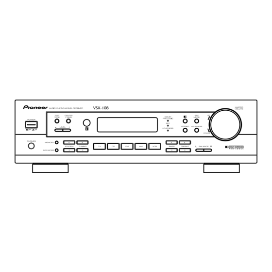
Page 35: Panel Facilities And Specifications
VSX-108 8. PANEL FACILITIES AND SPECIFICATIONS 8.1 PANEL FACILITIES Front Panel MASTER VOLUME POWER ON/OFF button PHONES JACK (Headphone terminal) TEST TONE ON/OFF button MPX MODE button The TEST TONE signal will be output in the Dolby Use to switch the auto stereo/monaural mode for Pro logic mode. - Page 36 VSX-108...
- Page 37 VSX-108 Display DIRECT LOUDNESS PRO LOGIC VIRTUAL DSP TAPE 2 MONO TUNED STEREO CHARACTER display TUNER indicator MONO: Lights when the monaural mode is set using the MPX MODE button. TUNED: Lights when broadcasts are being received. STEREO: Lights when stereo broadcasts are received during auto stereo mode.
- Page 38 VSX-108 Remote Control Unit FUNCTION button Use to switch the function setting of this unit. [TUNER operations] STATION -, +, BAND, TUNING -, +, MPX, D.ACCESS buttons. [TV operations] STANDBY/ON, CHANNEL -, +, TV FUNC., TV VOL. -, +, buttons [CD, TAPE, DVD, LD, VCR, MD operations] STANDBY/ON, 4, ¢...
-
Page 39: Specifications
VSX-108 8.2 SPECIFICATIONS Continous Power Output Accessories Front ......50 W + 50 W (1kHz, 0.9%, 8 ) Center ........50 W (1kHz, 0.9%, 8 ) Surround ......... 50 W (1kHz, 0.9%, 8 ) Input (Sensitivity/Impedance) CD, VCR / TV ........200 mV/47 k Frequency Response CD, VCR / TV ......