Table of Contents
Advertisement
Service
Manual
SR7000
SR8000
SECTION
1. TECHNICAL SPECIFICATIONS ................................................................................................................. 1
2. WIRING DIAGRAM ..................................................................................................................................... 3
3. BLOCK DIAGRAM ....................................................................................................................................... 5
4. SCHEMATIC DIAGRAM .............................................................................................................................. 7
5. PARTS LOCATION ................................................................................................................................... 31
6. IC DATA .................................................................................................................................................... 47
7. EXPLODED VIEW AND PARTS LIST ....................................................................................................... 53
8. SERVICE PROGRAM ............................................................................................................................... 56
9. ELECTRICAL ADJUSTMENTS ................................................................................................................. 58
10. ALIGNMENT PROCEDURES ................................................................................................................... 59
11. TROUBLE SHOOTING ............................................................................................................................. 61
12. TECHNICAL DESCRIPTION FOR DECODER ......................................................................................... 64
13. ELECTRICAL PARTS LIST ....................................................................................................................... 65
Please use this service manual with referring to the user guide ( D.F.U. ) without fail.
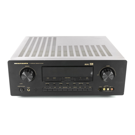
AV SURROUND RECEIVER SR7000
S U R R O U N D
CLEAR
MEMORY
6ch INPUT
A/D
S-DIRECT
STANDBY
POWER ON/STANDBY
PHONES
TV
LD
DVD
VCR1
AV SURROUND RECEIVER SR8000
S U R R O U N D
CLEAR
MEMORY
6ch INPUT
A/D
S-DIRECT
STANDBY
POWER ON/STANDBY
TV
LD
DVD
VCR1
PHONES
TABLE OF CONTENTS
SR7000 / SR8000
SR7000 /
SR8000 /
AV Surround Receiver
D I G I T A L
DOLBY
D I G I T A L
SURROUND
L
C
R
LFE
LS
S
RS
PEAK
DOWN
TUNING/PRESET
F/P
MODE
MULTI
SLEEP
DISPLAY OFF
MUTE
S-VIDEO
VIDEO
DSS/VCR2
AUX
CDR/MD
TAPE
CD
TUNER
D I G I T A L
DOLBY
D I G I T A L
SURROUND
L
C
R
LFE
LS
S
RS
PEAK
DOWN
TUNING/PRESET
F/P
MODE
MULTI
SLEEP
DISPLAY OFF
MUTE
S-VIDEO
VIDEO
DSS/VCR2
AUX
CDR/MD
TAPE
CD
TUNER
K1G, /N1G, /U1G
/K1B, /N1B, /U1B
K1G, /S1G, /U1B
VOLUME
UP
AUX INPUT
L
AUDIO
R
VOLUME
UP
AUX INPUT
L
AUDIO
R
PAGE
320J855010 MIT
3120 785 22280
First Issue 2000.02
R
Advertisement
Table of Contents

Related Manuals for Marantz SR8000


Summary of Contents for Marantz SR8000
- Page 1 AUDIO PHONES VCR1 DSS/VCR2 CDR/MD TAPE TUNER SR8000 D I G I T A L AV SURROUND RECEIVER SR8000 DOLBY D I G I T A L SURROUND S U R R O U N D VOLUME PEAK DOWN TUNING/PRESET...
- Page 2 MARANTZ Parts for your equipment are generally available to our National Marantz Subsidiary or Agent. ORDERING PARTS : Parts can be ordered either by mail or by Fax.. In both cases, the correct part number has to be specified.
-
Page 3: Technical Specifications
Power Consumption ............360W Dimension ( MAX ) Width ..........17-1/4 inches (440 mm) Width (SR8000 U only) ......18 inches (458 mm) Height ........... 6-1/4 inches (159 mm) Depth ..........18-1/8 inches (460 mm) Weight (SR7000) ........33.1 lds. (14.5 kg) Weight (SR8000) ........... -
Page 4: Subwoofer Output
Remark : Bass signal output from Sub Woofer terminal for SR7000/SR8000 Sub woofer output is not active while all surround modes. Please refer to the following table. SubWoofer Output SPK setup Dolby Digital Dolby Hall , Matrix Stereo Source (Pro Logic) - Page 5 2. WIRING DIAGRAM PH 3P PH 2P PH 5P WL01 JX06 JL06 JQ06 PL04 P904 PL54 PS54 PS04 PL74 P104 J901 JX05 JX04 JL04 JL05 JQ05 JQ04 JS04 JS03 J105 MQ 8P MQ 5P MQ 10P MQ 12P MQ 12P MQ 7P MQ 12P MQ 8P...
- Page 6 FUNCTION RDS DATA LC72722 HEADPHONE MULTI PRE OUT KILL RDS INDIVIDUAL & MASTER (ONLY S,N) MAIN TAPE SPK OUTPUT ELE.-VOL. X6CH TC9482 SR8000 ONLY HDAM FRONT FRONT MAIN MUTE CONTROL 6CH DIR/STEREO MULTI ROOM LC78212 CENTER MAIN AUDIO OUT QG57 CENTER ELE.
- Page 7 +5VC TUNER 2SC536 SU23 SU22 SU21 SU20 SU19 SU18 SU17 SU16 5V-4 CENTER S EC-A DU04 RU45 RU91 OPEN SR8000 OPEN SP/ETC HLMF-K2 +5VB LED-ST 5V-3 SU81 DU03 RU46 1k OHM SR7000 10k OHM HLMF-K2 +5VB +5VB 5V-3 5V-3 +5VB...
- Page 8 50µs DE-EMPHASIS TUNING VOLTAGE (OTHER)-A101 5pin 9kHz /SCAN STEP SW. C309 87.5MHz 108MHz K ONLY 0.015 P104 2.1V 7.2V 520/531kHz 1710/1602kHz 1.1V 7.6V Tuner P.C.Board C310 75µs 0.015 TUNING VOLTAGE (F)-A101 5pin S301 10kHz 76.0MHz 90MHz RTU-*A,1,2,3,5** 4.0V 531kHz 1602kHz 1.1V 6.9V L301...
- Page 9 -15V CS13 -15V-3 CS01 Audio selector(Audio) P.C.Board 10/50V AUDIO SELECTOR(AUDIO SOURCE) PS04 +15V RS13 15V-2 RS07 JS01 RRJ-*S** NJM4558M RS01 QS01 RS14 4558MD RRM-*S5* RS02 RS08 CS14 CS15 CS02 RS09 +15V 10/50V 15V-2 RS23 -15V RS03 CS03 100K CS29 -15V-3 10/50V RS15 RS04...
- Page 10 Videoo selector(CVBS) P.C.Board PL04 QL65 XL61 DTC114TS /UN4215 SR8000 ONLY 14.31818MHz 5V-34 DY61 0/4.6 /KRC111M RVC-*L** K,N,S ONLY DAN202K QL64 DTC114TS MULTI OSD CONTROL RRL-*L6* /UN4215 QL66 /KRC111M DY62 5V-34 0/5.0 DTA114ES 2.8/0 K,N,S ONLY /UN4111 DAN202K XL62 /KRA102M RCN-*Y6* RL69 17.31818MHz...
- Page 11 FRONT-L POWER AMP R739 P704 22 1/4W 5ch Power Amp P.C.Board D701 D715 R729 C725 R717 C715 100P/500V Q715 220/63V 52.3 51.6 2SC4793 Q721 Q709 R743 51.6 D703 D717 2SC5200 RMA-*7,P,T** 2SA1360 Q705 51.0 R753 51.0 2SA1145 R773 R759 HSS81 R719 1.2k D705...
- Page 12 FRONT L CM65 -15VE CM69 100/25V CC07 RC07 6ch/Preout P.C.Board +15VE 22/50V FRONT L QM59 15V-2 6CH FL RM59 QM55 2SC2705 SR8000 RC13 CC20 QC01 6CH DIRECT IN 100K 0.01 NJM2068M 15.0 +15VE QM51 JC01 15V-2 2SA970 CM51 RM51 RG49...
- Page 13 RCR-XCXX RVR-XGXX -15V-3 -15VE PG04 CC07 RC07 22/50V FRONT L FRONT L 6CH FL 6ch/Preout P.C.Board RC13 CC20 QC01 100K 0.01 NJM2068M RG58 CG13 6CH DIRECT IN +15VE 3.9K +15VE SR7000 CG07 JC01 15V-2 15V-2 33/25V CG01 CM69 CM70 FRONT-L RC01 CC08 RG13...
- Page 14 0V-2 DTC114ES 0.01 /UN4211 500V 1/4W /KRC102M 0V-4 0V-4 CY14 RY13 62V-10 C802 RN08 100K 0.01 J825 0V-2 15K 1/2W SR8000:27000/63V 0V-5 0V-4 RY19 J823 J821 J827 QY10 100K CY07 SR7000:15000/63V LY02 NJM4558DD 10/50V D801 +5VD 0V-2 RN03 C803 RN02...
- Page 15 CD68 Q691 0.01 NC17 N.C. C694 +5VD C693 100/10V N.C. SUB-CPU LD58 CD61 QD51 R694 CD77 CD60 CD59 JR06 (SR8000 ONLY) 5V-20 CD69 0.022 0.01 BA033FP +5VD ISEL1 ISEL2 ISEL3 220/10V 0.01 100/10V 0.01 +5VD ISEL1 5V-20 5V-20 +5VD DIGITAL...
- Page 16 W602 P604-2/2 W602A W602B DSP P.C.Board W601 SW Mix F SW Mix S SR8000 W601A W601B 1kHz,0dB=1.94V 30Hz,0dB=3.64V 30Hz,0dB=1.97V 0V-8 1kHz,0dB=1.333V -15VAD DD01 CH13 -15V-37 ISS300 -15VAD CH15 -15V-37 RDD-*D,H,J** FRONT Lch 1kHz,0dB=1.886V RD04 RH29 0V-10 RH21 0V-10 RH17 5V-20 +5VD 1kHz,0dB(-3dBdown)=0.70V...
- Page 17 P604-2/2 W601 SW Mix F SW Mix S DSP P.C.Board W601A W601B SR7000 0V-8 RDD-*D,H,J** 1kHz,0dB=1.94V 30Hz,0dB=3.27V 30Hz,0dB=1.78V RH35 CH29 1kHz,0dB=1.886V RH29 NOIZE(20KHZ) =2.16UV RH21 RH19 Noize(A-Weig)=1.80uV CH13 RH07 RDA-*K** -15VAD 1kHz,0dB=0.75V THD=0.0005% -15V-37 CK20 CH03 RH11 FRONT Lch CH11 RH13 RH27 22/50V...
- Page 18 P904 Remote I/O P.C.Board J902 R901 +5.6VL 5.6V-8 RRN-*9** C905 0.01 C906 Q901 0 OHm DTA114ES /UN4111 Q902 R903 /KRA102M J903 PC817 J901 R905 R904 C907 08MQ-ST-L 0.01 TO JY11(PY04) C909 C908 RC-5 IN/OUT 0 OHm 0.01 MURTI RC IN Q904 Q905 DTA114ES...
- Page 19 P104 (COMPONENT SIDE VIEW) Q203 Q501 5. PARTS LOCATION Q201 Q204 Q351 Q202 Q354 QA02 QA01 QA04-QA06 Q352 353 P904 (COMPONENT SIDE VIEW) Q901 Q904 Q903 Q907 Q908 Q906 P904 (COPPER SIDE VIEW) P104 (COPPER SIDE VIEW) Q301...
- Page 20 PL04 (COMPONENT SIDE VIEW) QL64-QL66 QL62 PL54 (COMPONENT SIDE VIEW) QX07-QX09 QL07-QL09 QL63 QL67 QX05 QX06 QX10 QL10 QY61 QL05 QL06 PL04 (B) QL61 QL03 QL68 QL01 QL02 (B) : (COPPER SIDE VIEW) PL54 (B) QX01 - QX04 QX11...
- Page 21 PG04 (COMPONENT SIDE VIEW) QM57 QM53 QM59 QM55 QM51 QG01 QC04 PB04 ( U ONLY ) QM58 QM54 QM60 QB03 QM56 QM52 QB04 QB02 QB01 CB07 CB06 JB05 RB01 CB09 8A/125V JB06 JB07 QB04 CB05 FB01 U194 CB11 DB11 U093 U195 RB05 RB11...
- Page 22 PS04 (COMPONENT SIDE VIEW) QS04 PS54 (COMPONENT SIDE VIEW) QQ07 QS51 QQ06 QS54 QS55-QS58 QS59 PS04 (B) QS01 - QS03 QS52 PS54 (B) QQ01 - QQ05 QQ08 (B) : (COPPER SIDE VIEW) QS52...
- Page 23 P604 (COMPONENT SIDE VIEW) QJ12 QJ07 QJ06 QJ11 QJ04 QJ02 Q601 QR06 QJ05 QJ01 Q604 QR01 QR08 QR02 QD01 QH02 Q602 QR03 QK04 Q691 QR07 QH01 QK01 QR04 QJ08 QJ09 QK07 QK056 QK02 QD51...
- Page 24 ALL COPPER SIDE VIEW P704 QP03 QP01 QP09 QP05 Q704 Q702 Q710 Q706 QP04 QP04 QP10 QP06 QT03 QT01 QT09 QT05 Q703 Q701 Q709 Q705 QP07 QP11 Q708 Q712 QP04 QP14 QT07 QT11 Q707 Q711 WA321J1012 SURR. L 5CH POWER AMP FRONT R SURR.
- Page 25 ALL COPPER SIDE VIEW PY04 QY03 - QY08 QY11 - QY13 QY01 QY02 QY09 QY10 QN02 - QN06 Q821 - Q823 Q824 QN01 U008 RY05 DY01 MR-O U009 MR-I U029 DY05 U010 JY34 +15V DY06 U030 +5VL U260 TU-L TU-L RY06 U031 DY02...
- Page 26 VCR1 RU25 RU28 RU23 RU24 RU26 RU30 RU08 CU08 CU09 PU44 SU16 SU17 SU18 SU19 SU20 SU21 SU22 SU23 SU06 SU07 QU18 CU82 RU84 QU82 RU83 RU86 RU81 RU82 CU81 U122 ( SR8000 ONLY ) HDAM U123 DU81 PU54 SU91...
- Page 27 6. IC DATA Q601:YSS912 NAME I/O FUNCTION NAME I/O FUNCTION VDD1 +5V power supply (for I/Os) VDD2 +3.3V power supply (for core logic) RAMCEN O External SRAM Interface /CE 52 NONPCM O Detection of non PCM data. (Refer to " Status Register") RAMA16 O External SRAM Interface address 16 O Detection of AC-3 CRC error.
- Page 28 QK04:AK4526 QL04,QL62,QX06:LC74781 No. Pin Narne I/O Function No. Pin Name I/O Function SDOS SDTO Source Select Pin LOUT3 O Lch #3 analog output pin L: Internal ADC output, "H": DAUX input ROUT3 O Rch #3 analog output pin LOUT2 O Lch #2 analog output pin Ored with serial control register if P/S="L".
- Page 29 Q501:LC72130 QY01:TMP93CW40DF Q691: PD78018 Pin Port name Sig.Name Act. Note Port name USE Sig. Name act. Description 1 P55/AN5 KEY_INPUT3 Key Input 3 1 P30/TO0 C0_E0 DIR Status 2 P56/AN6 MODE_SW0 MODE SWITCH 0 REFERENCE PHASE DETECTOR 2 P31/TO1 Ca_E1 DIR Status X IN DIVIDER...
- Page 30 7. EXPLODED VIEW AND PARTS LIST S V E RS ION Z 0 0 7 K & S V E RS ION N V E RS I ON J 0 0 1 K V E RS I ON Z 0 0 7 5 1 2 8 0 0 4 D( K &...
- Page 31 MASK IR 312J303030 FOR SR7000 ( Lot number 033B 996500001393 LENS STANDBY LENS 312J355010 from 01 to 12 ) and SR8000 034B /K,/N,/S 996500001394 JOINT POWER 312J125010 ( Lot number from 01 to 09 ) 035B BLACK 996500001975 BUTTON POWER SW BLACK...
- Page 32 8. SERVICE PROGRAM REMARK If these service programs are set, All user preset memories will be cleared. 1. FACTORY mode (Tracking point memory) This FACTORY mode can be use for measurement of the tuner circuit. When the product is POWER ON, press both [ MEMO ] and [ F/P ] buttons simultaneously over 3 seconds. FLD shows "FACTORY"...
- Page 33 Fig 2. Input selection order by pressing [ MODE] button each time ORDER INDICATION for INPUT STATUS AUTO D1 DIG. 1 IN AUTO D2 DIG. 2 IN AUTO D3 DIG. 3 IN AUTO D4 DIG. 4 IN DIG. 5 IN AUTO D5 DIG.
- Page 34 9. ELECTRICAL ADJUSTMENTS 1. DC offset adjustment Master Volume : Minimum, Speaker out : non Load Adjustment Step Power Channel Test Point Adjustment Vaule Point Front L R767 Center RT67 Speaker Output ± Front R R768 20mV Terminal Surr. L RP67 Surr.
- Page 35 10. ALIGNMENT PROCEDURES 1. AM IF Adjustment Input Signal Source Signal Source Signal Output Reception Adjustment Adjustment Step Connection Frequency Level and Modulation Frequency Point Value 999 kHz Output level Signal generator output to (K, S, N) Level 300 V/m (50dB/m) (L or R) transmission *loop antenna.
- Page 36 6. FM Muting Level Adjustment Turn the variable resistor R212 to no indication ("TUNED") point. And return that valuable resistor in opposite to the "TUNED" indicate point. Input Signal Source Signal Source Signal Output Reception Adjustment Adjustment Step Connection Frequency Level and Modulation Frequency Point...
-
Page 37: Trouble Shooting
11. TROUBLE SHOOTING No Power Standby Power supply circuite (PB04) LED Lights up on has any problem. standby mode To be check +5VL or PDOWN signal. FLD shows Vkk or FL is not supplied ERROR PWR1 to PU04 Supply +24V to PU04? Can PY04 supply +24V ? - Page 38 No sound from SPK on Analog Stereo mode Test Tone is OK ? Analog S-Direct is Pre output is OK ? active ? (Volume, & Power Amp are P704, P754 (Volume , Power Amp & Volume, HDAM , QC04 or SPK Relay Audio Input are OK) or Preout Relay has problem...
- Page 39 No sound from SPK on AC-3/DTS decode Volume, HDAM, QC04 6ch Direct or Preout Relay is OK ? has any trouble.(PG04) P604 has trouble DD,DTS,PCM DIR(QR01) or Q601 Pre output is Test tone is are shown? OK ? has trouble OK ? DAC &...
- Page 40 6 channel analog audio signals (Front L/R SURROUND L/R, CENTER, LEF) are coverted from output data of DSP. Digital signal is converted from analog audio input for Pro Logic or other effect mode. SUB CPU (Q691:uPD78018FGC) This chip controls ICs in P604 and comunicate with QU01. Connect to QU01 with serial interface lines. : SR8000 only...
-
Page 41: Electrical Parts List
13. ELECTRICAL PARTS LIST NOTE ON SAFETY FOR FUSIBLE RESISTOR : ASSIGNMENT OF COMMON PARTS CODES. RESISTORS The suppliers and their type numbers of fusible resistors : 1) GD05 × × × 140, Carbon film fixed resistor, ±5% 1/4W are as follows; : 2) GD05 ×... - Page 42 VERS. PART NO. VERS. POS. POS. PART NO. PART NO. PART NO. DESCRIPTION DESCRIPTION COLOR (FOR PCS) COLOR (FOR PCS) (MJI) (MJI) P101-FM AM TUNER C503 482212490353 ELECT. 100µF M 10V RA-2 OA10701020 CIRCUIT BOARD C504 532212234098 CER. CHIP 0.01µF DK56103300 P101-CAPACITORS C505...
- Page 43 VERS. PART NO. VERS. POS. POS. PART NO. PART NO. PART NO. DESCRIPTION DESCRIPTION COLOR (FOR PCS) COLOR (FOR PCS) (MJI) (MJI) R321 /U 482211190892 CHIP 0 ±5% 1/10W NI05000110 QA05 /N 482213061227 DIG.TRS. BA10001000 R322 /U 482211190892 CHIP 0 ±5% 1/10W NI05000110 DTA114ES UN4111 10K 10K R323...
- Page 44 VERS. PART NO. VERS. POS. POS. PART NO. PART NO. PART NO. DESCRIPTION DESCRIPTION COLOR (FOR PCS) COLOR (FOR PCS) (MJI) (MJI) C693 482212611687 CER. CHIP 0.1µF DK98104200 CJ53 8000 FILM 0.001µF J M 50V DF15102350 C694 482212490353 ELECT. 100µF 10V OA10701020 CJ54 8000 FILM 0.27µF J 50V...
- Page 45 VERS. PART NO. VERS. POS. POS. PART NO. PART NO. PART NO. DESCRIPTION DESCRIPTION COLOR (FOR PCS) COLOR (FOR PCS) (MJI) (MJI) CR18 482212611687 CER. CHIP 0.1µF DK98104200 RH18 8000 482211683819 CHIP 18k 1/16W NN05183610 CR20 532212611583 CER. CHIP 0.01µF 50V DK96103200 RH19 482211712925 CHIP 47k 1/16W...
- Page 46 VERS. PART NO. VERS. POS. POS. PART NO. PART NO. PART NO. DESCRIPTION DESCRIPTION COLOR (FOR PCS) COLOR (FOR PCS) (MJI) (MJI) RJ67 482205130221 CHIP 220 1/16W NN05221610 RR15 482205130103 CHIP 10k 1/16W NN05103610 RJ67 8000 482205130392 CHIP 3.9k 1/16W NN05392610 RR16 482205130759 CHIP 75 1/16W...
- Page 47 VERS. PART NO. VERS. POS. POS. PART NO. PART NO. PART NO. DESCRIPTION DESCRIPTION COLOR (FOR PCS) COLOR (FOR PCS) (MJI) (MJI) QR08 482220933519 IC TC7W74F HC10381050 CP15 482212423068 ELECT. 220µF 63V M RA-2 OA22706320 P604-MISCELLANEOUS CP18 J691 PLUG SOCKET 12P 12MQ-ST-L YP06902090 CP19 482212411533 ELECT.
- Page 48 VERS. PART NO. VERS. POS. POS. PART NO. PART NO. PART NO. DESCRIPTION DESCRIPTION COLOR (FOR PCS) COLOR (FOR PCS) (MJI) (MJI) RP09 482205022202 2.2k ±5% 1/6W GG05222160 P704-SEMICONDUCTORS RP10 482205022202 2.2k ±5% 1/6W GG05222160 D701 RP13 482205022202 2.2k ±5% 1/6W GG05222160 482213032362 DIODE 1SS176 MA165 1SS254 HD20002000 RP14...
- Page 49 VERS. PART NO. VERS. POS. POS. PART NO. PART NO. PART NO. DESCRIPTION DESCRIPTION COLOR (FOR PCS) COLOR (FOR PCS) (MJI) (MJI) Q723 482213063119 TRS. 2SA1943 R OR O HT119432A0 KP16 TRS. KIT 2SA1837 2SC4793 HK183719C0 230V 15A 150W HFE SELECTED RANK Q724 482213063119 TRS.
- Page 50 VERS. PART NO. VERS. POS. POS. PART NO. PART NO. PART NO. DESCRIPTION DESCRIPTION COLOR (FOR PCS) COLOR (FOR PCS) (MJI) (MJI) R912 482211711449 CHIP 2.2k ±5% 1/10W NI05222110 QB03 /U 482220973674 IC NJM7806FA +6W 1A HC38906090 R913 996500003408 VAR. RK09D111 20k B RK02031090 QB04 /U 482220914883 IC S-806C...
- Page 51 VERS. PART NO. VERS. POS. POS. PART NO. PART NO. PART NO. DESCRIPTION DESCRIPTION COLOR (FOR PCS) COLOR (FOR PCS) (MJI) (MJI) PG04-5CH E-VR PRE-OUT CG32 /N,/S 532212234099 CER. CHIP 470pF DK56471300 CIRCUIT BOARD CG33 /K,/U 532212610794 CER. CHIP 220pF DK56221300 PG04-CAPACITORS CG33 /N,/S...
- Page 52 VERS. PART NO. VERS. POS. POS. PART NO. PART NO. PART NO. DESCRIPTION DESCRIPTION COLOR (FOR PCS) COLOR (FOR PCS) (MJI) (MJI) RG07 482211710833 CHIP 10k 1/10W NI05103110 DM51 8000 996500003401 CHIP DIODE RB425D HZ20030210 RG07 8000 482211190892 0k 1/10W NI05000110 DM52 8000 996500003401 CHIP DIODE RB425D...
- Page 53 VERS. PART NO. VERS. POS. POS. PART NO. PART NO. PART NO. DESCRIPTION DESCRIPTION COLOR (FOR PCS) COLOR (FOR PCS) (MJI) (MJI) CL35 532212232658 CER. CHIP 22pF DD55220300 RL15 482211710833 CHIP 10k ±5% 1/10W NI05103110 CL36 482212611591 CER. CHIP 24pF J CH 50V BLK DD15240300 RL16 482205120822 CHIP 8.2k ±5% 1/10W NI05822110...
- Page 54 VERS. PART NO. VERS. POS. POS. PART NO. PART NO. PART NO. DESCRIPTION DESCRIPTION COLOR (FOR PCS) COLOR (FOR PCS) (MJI) (MJI) QL66 8000 482213061227 DIG.TRS. BA10001000 CX54 532212421731 ELECT. 10µF M 50V RA-2 OA10605020 /K,/S DTA114ES/UN4111 10K 10K CX55 532212421731 ELECT.
- Page 55 (FOR PCS) COLOR (FOR PCS) (MJI) (MJI) QX08 /K,/N,/S 482213061189 DIG.TRS. BA20004000 PM01-HDAM CIRCUIT BOARD DTC114TS UN4215 10K [SR8000 ONLY] QX09 /K,/N,/S 482213061227 DIG.TRS. BA10001000 PM01-RESISTORS (COMMON) DTA114ES UN4111 10K 10K 8000 CARBON FILM FIXED RES. QX10 482213041947 TRS. 2SC536SP ETC HT30001000 ±5% 1/6W : ALL...
- Page 56 VERS. PART NO. VERS. POS. POS. PART NO. PART NO. PART NO. DESCRIPTION DESCRIPTION COLOR (FOR PCS) COLOR (FOR PCS) (MJI) (MJI) CS60 532212421731 ELECT. 10µF M 50V RA-2 OA10605020 QS04 482220932552 IC LC78211 HC10308030 CS61 532212234098 CER. CHIP 0.01µF DK56103300 QS51 482220931618 IC LC7536...
- Page 57 VERS. PART NO. VERS. POS. POS. PART NO. PART NO. PART NO. DESCRIPTION DESCRIPTION COLOR (FOR PCS) COLOR (FOR PCS) (MJI) (MJI) CQ41 CU15 482212423056 ELECT 47µF 10V EJ47601010 482212233127 CER. CHIP 2200pF DK56222300 CU16 482212490406 BIG ELECT CAP EX22300530 CQ44 FMOH223ZTP16 SUPER CQ45...
- Page 58 VERS. PART NO. VERS. POS. POS. PART NO. PART NO. PART NO. DESCRIPTION DESCRIPTION COLOR (FOR PCS) COLOR (FOR PCS) (MJI) (MJI) PU44-SUB FRONT CN03 482212240617 CER. 0.1µF +80%-20% 50V DC DD38104010 CIRCUIT BOARD CN04 482212441539 ELECT. 47µF M 16V RA-2 OA47601620 PU44-CAPACITORS CN05...
- Page 59 VERS. POS. PART NO. PART NO. DESCRIPTION COLOR (FOR PCS) (MJI) Q825 482220930258 IC NJM7905FA HC39905090 QN01 482220983312 IC TA7317P HC10042050 QN02 482213042594 DIG.TRS. BA20002000 DTC144ES UN4213 47K 47K QN03 482213042949 TRS. 2SA970 GR OR BL HT109702A0 QN04 482213060696 TRS. 2SC1627 O Y 8 HT316272B0 0V 300MA 600MW TO QN05...