Table of Contents
Advertisement
Quick Links
®
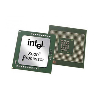
Intel
Xeon
and 7300 Series
Datasheet
September 2008
®
Notice: The Intel
Xeon
as errata which may cause the product to deviate from published specifications. Current characterized errata are
available on request.
®
Processor 7200 Series
®
Processor 7200 Series and 7300 Series may contain design defects or errors known
Document Number: 318080-002
Advertisement
Table of Contents

Related Manuals for Intel BFCBASE - Motherboard - 7300


Summary of Contents for Intel BFCBASE - Motherboard - 7300
- Page 1 Datasheet September 2008 ® ® Notice: The Intel Xeon Processor 7200 Series and 7300 Series may contain design defects or errors known as errata which may cause the product to deviate from published specifications. Current characterized errata are available on request.
- Page 2 Current characterized errata are available on request. Contact your local Intel sales office or your distributor to obtain the latest specifications and before placing your product order. Copies of documents which have an ordering number and are referenced in this document, or other Intel literature may be obtained by calling 1-800-548-4725 or by visiting Intel's website at http://www.intel.com.
-
Page 3: Table Of Contents
Contents Introduction ......................9 Terminology ..................... 11 State of Data ....................13 References ....................... 13 Electrical Specifications ................... 15 Front Side Bus and GTLREF ................15 Decoupling Guidelines ..................15 2.2.1 VCC Decoupling..................16 2.2.2 VTT Decoupling ..................16 2.2.3 Front Side Bus AGTL+ Decoupling ............ - Page 4 7.2.3 Stop-Grant State .................. 114 7.2.4 Extended HALT Snoop or HALT Snoop State, Stop Grant Snoop State ..................115 Enhanced Intel SpeedStep® Technology ............. 115 System Management Bus (SMBus) Interface ............116 7.4.1 SMBus Device Addressing ..............117 7.4.2 PIROM and Scratch EEPROM Supported SMBus Transactions....... 118 7.4.3...
- Page 5 Figures Quad-Core Intel® Xeon® L7345 Processor Load Current versus Time ..... 27 Dual-Core Dual-Core Intel® Xeon® Processor 7200 Series Load Current versus Time...................... 28 ® ® Quad-Core Intel Xeon Processor 7200 Series and 7300 Series Load Current versus Time28 Quad-Core Intel® Xeon® X7350 Processor Load Current versus Time ....29 ®...
- Page 6 Quad-Core Intel® Xeon® L7345 Processor Thermal Specifications ......99 Quad-Core Intel® Xeon® L7345 Processor Thermal Profile........100 Dual-Core Intel® Xeon® Processor 7200 Series Thermal Specifications ....101 Dual-Core Intel® Xeon® Processor 7200 Series Thermal Profile......102 BREQ# signal assertion during power on............. 109 6-10 PECI Address assigned to processor ..............
- Page 7 Extended HALT Maximum Power................ 113 Memory Device SMBus Addressing..............118 Read Byte SMBus Packet .................. 118 Write Byte SMBus Packet ................. 118 Processor Information ROM Data Sections ............119 128 Byte ROM Checksum Values ............... 137 Document Number: 318080-002...
-
Page 8: Revision History
-001 • Initial Release September 2007 ® ® 318080 -002 • Changed Product Name to Intel Xeon Processor 7200 Series and September 2008 7300 Series • Updated Power Specifications • The character byte ordering was reversed for the following fields:... -
Page 9: Introduction
The 1066 MHz Front Side Bus (FSB) is a quad-pumped bus running off a 266 MHz system clock ® making 8.5 GBytes per second data transfer rates possible. The Quad-Core Intel ® Xeon X7350 processor offers higher clock frequencies than the other Quad-Core ®... -
Page 10: Quad-Core Intel® Xeon® Processor 7300 Series Processor Features
Virtualization Technology is a set of hardware enhancements that can improve virtualization solutions. Intel Virtualization Technology is used in conjunction with Virtual Machine Monitor software enabling multiple, independent software environments inside a single platform. Further details on Intel Virtualization Technology can be found at http://developer.intel.com/technology/vt. ®... -
Page 11: Terminology
FSB speeds and bandwidth. • Flexible Motherboard Guidelines (FMB) – Are estimates of the maximum values the Intel® Xeon® Processor 7200, 7300 Series will have over certain time periods. The values are only estimates and actual specifications for future processors may differ. - Page 12 64 – Instruction set architecture and programming environment of Intel’s 64-bit processors, which are a superset of and compatible with IA-32. This 64-bit ® instruction set architecture was formerly known as IA-32 with EM64T or Intel EM64T. • Platform Environment Control Interface (PECI) – A proprietary one-wire bus...
-
Page 13: State Of Data
Introduction State of Data This document contains preliminary information on new products in production. The specifications are subject to change without notice. Verify with your local Intel sales office that you have the latest datasheet before finalizing a design References... - Page 14 Introduction Document Number: 318080-002...
-
Page 15: Electrical Specifications
) for AGTL+ signals are provided on the processor silicon and are terminated to VTT. The on-die termination resistors are always enabled on the processor to control reflections on the transmission line. Intel chipsets also provide on-die termination, thus eliminating the need to terminate the bus on the baseboard for most AGTL+ signals. -
Page 16: Vcc Decoupling
Electrical Specifications remains within the specifications listed in Table 2-9. Failure to do so can result in timing violations or reduced lifetime of the component. For further information and guidelines, refer to the appropriate platform design guidelines. 2.2.1 Decoupling Vcc regulator solutions need to provide bulk capacitance with a low Effective Series Resistance (ESR). -
Page 17: Front Side Bus Frequency Select Signals (Bsel[2:0])
Individual processors operate only at or below the frequency marked on the package. Listed frequencies are not necessarily committed production frequencies. For valid processor core frequencies, refer to the Dual-Core Intel® Xeon® Processor 7200 Series and Quad-Core Intel® Xeon® Processor 7300 Series Specification Update. - Page 18 Dual-Core Intel® Xeon® Processor 7200 Series and Quad-Core Intel® Xeon® Processor 7300 Series. The Dual-Core Intel® Xeon® Processor 7200 Series and Quad-Core Intel® Xeon® Processor 7300 Series provides the ability to operate while transitioning to an adjacent VID and its associated processor core voltage (V ).
-
Page 19: Voltage Identification Definition
Notes: When this VID pattern is observed, the voltage regulator output should be disabled. Shading denotes the expected VID range of the Dual-Core Intel® Xeon® Processor 7200 Series and Quad-Core Intel® Xeon® Processor 7300 Series. The VID range includes VID transitions that may be initiated by thermal events, assertion of the FORCEPR# signal (see ®... -
Page 20: Reserved, Unused, Or Test Signals
Electrical Specifications Reserved, Unused, or Test Signals All Reserved signals must remain unconnected. Connection of these signals to V , or to any other signal (including each other) can result in component malfunction or incompatibility with future processors. See Section 4 for a pin listing of the processor and the location of all Reserved signals. -
Page 21: Fsb Signal Groups
Electrical Specifications Table 2-4. FSB Signal Groups Signal Group Type Signals AGTL+ Common Clock Input Synchronous to BCLK[1:0] BPRI#, DEFER#, RESET#, RS[2:0]#, RSP#, TRDY#; AGTL+ Common Clock Output Synchronous to BCLK[1:0] BPM4#, BPM[2:1]#, BPMb[2:1]# AGTL+ Common Clock I/O Synchronous to BCLK[1:0] ADS#, AP[1:0]#, BINIT# , BNR# , BPM5#,... -
Page 22: Cmos Asynchronous And Open Drain Asynchronous Signals
Electrical Specifications Table 2-5 outlines the signals which include on-die termination (R Table 2-6 outlines non AGTL+ signals including open drain signals. Table 2-7 provides signal reference voltages. Table 2-5. AGTL+ Signal Description Table AGTL+ signals with R AGTL+ signals with no R A[39:3]#, ADS#, ADSTB[1:0]#, AP[1:0]#, BINIT#, BPM[5:0]#, BPMb[3:0]#, RESET#, BR[1:0] BNR#, BPRI#, D[63:0]#, DBI[3:0]#, DBSY#,... -
Page 23: Mixing Processors
FSB frequency, core frequency, number of cores, and have the same internal cache sizes. Mixing components operating at different internal clock frequencies or number of cores is not supported and will not be validated by Intel. Note: Processors within a system must operate at the same frequency per bits [12:8] of the CLOCK_FLEX_MAX MSR;... -
Page 24: Processor Dc Specifications
Electrical Specifications 2.11 Processor DC Specifications The following notes apply: • The processor DC specifications in this section are defined at the processor die and not at the package pins unless noted otherwise. • The notes associated with each parameter are part of the specification for that parameter. -
Page 25: Flexible Motherboard Guidelines (Fmb)
Flexible Motherboard Guidelines (FMB) The Flexible Motherboard (FMB) guidelines are estimates of the maximum values the Dual-Core Intel® Xeon® Processor 7200 Series and Quad-Core Intel® Xeon® Processor 7300 Series will have over certain time periods. The values are only estimates and actual specifications for future processors may differ. Processors may or may not have specifications equal to the FMB value in the foreseeable future. - Page 26 V stable for V supply after V stable Thermal Design Current (TDC) Quad- 6,14 CC_TDC Core Intel® Xeon® L7345 Processor Launch - FMB Thermal Design Current (TDC) Dual- 6,14 CC_TDC Core Intel® Xeon® Processor 7200 Series Launch - FMB ®...
-
Page 27: Quad-Core Intel® Xeon® L7345 Processor Load Current Versus Time
CC_RESET RESET# de-assertion time specification and Table 2-23 for the RESET# Pulse Width specification. Figure 2-1. Quad-Core Intel® Xeon® L7345 Processor Load Current versus Time 0.01 1000 Tim e Duration (s) Notes: Processor or Voltage Regulator thermal protection circuitry should not trip for load currents greater than CC_TDC Not 100% tested. -
Page 28: Dual-Core Dual-Core Intel® Xeon® Processor 7200 Series Load Current Versus Time
Electrical Specifications Figure 2-2. Dual-Core Dual-Core Intel® Xeon® Processor 7200 Series Load Current versus Time 10 0 0 . 0 1 0 . 1 10 0 10 0 0 Tim e Duration (s) Notes: Processor or Voltage Regulator thermal protection circuitry should not trip for load currents greater than CC_TDC Not 100% tested. -
Page 29: Quad-Core Intel® Xeon® X7350 Processor Load Current Versus Time
Electrical Specifications Figure 2-4. Quad-Core Intel® Xeon® X7350 Processor Load Current versus Time 13 0 12 5 12 0 10 5 10 0 0 . 0 1 0 . 1 10 0 10 0 0 Tim e Duration (s) Notes:... - Page 30 Regulator Module (VRM) and Enterprise Voltage Regulator Down (EVRD) 11.0 Design Guidelines for socket load line guidelines and VR implementation. Please refer to the appropriate platform design guide for details on VR implementation. values greater than 60 A are not applicable for the Quad-Core Intel® Xeon® L7345 Processor. ® ®...
-
Page 31: Tolerance Load Lines
Electrical Specifications ® ® Figure 2-5. Quad-Core Intel Xeon Processor 7200 Series and 7300 Series V Static and Transient Tolerance Load Lines Icc [A] VID - 0.000 VID - 0.020 Maximum VID - 0.040 VID - 0.060 VID - 0.080 VID - 0.100... -
Page 32: Quad-Core Intel® Xeon® X7350 Processor Vcc Static And Transient Tolerance Load Lines
Electrical Specifications Figure 2-6. Quad-Core Intel® Xeon® X7350 Processor VCC Static and Transient Tolerance Load Lines Icc [A ] 100 105 110 115 120 125 130 V ID - 0.000 M ax im um V ID - 0.050 V ID - 0.100 V ID - 0.150... -
Page 33: Quad-Core Intel® Xeon® L7345 Processor
Electrical Specifications Figure 2-7. Quad-Core Intel® Xeon® L7345 Processor V Static and Transient Tolerance Load Lines Icc [A] VID - 0.000 VID - 0.010 Maximum VID - 0.020 VID - 0.030 VID - 0.040 VID - 0.050 VID - 0.060 VID - 0.070... -
Page 34: Tolerance Load Lines
Electrical Specifications Figure 2-8. Dual-Core Intel® Xeon® Processor 7200 Series V Static and Transient Tolerance Load Lines Icc [A] VID - 0.000 VID - 0.020 Maximum VID - 0.040 VID - 0.060 VID - 0.080 VID - 0.100 VID - 0.120 Typical VID - 0.140... -
Page 35: Platform Environmental Control Interface (Peci) Dc Specifications
Platform Environmental Control Interface (PECI) DC Specifications PECI is an Intel proprietary one-wire bus interface that provides a communication channel between Intel processor and external thermal monitoring devices. The Dual- Core Intel® Xeon® Processor 7200 Series and Quad-Core Intel® Xeon® Processor... -
Page 36: Peci Dc Electrical Limits
Electrical Specifications 7300 Series contains Digital Thermal Sensors (DTS) distributed throughout the die. These sensors are implemented as analog-to-digital converters calibrated at the factory for reasonable accuracy to provide a digital representation of relative processor temperature. PECI provides an interface to relay the highest DTS temperature within a die to external management devices for thermal/fan speed control. -
Page 37: Vcc Overshoot Specification
Electrical Specifications Figure 2-9. Input Device Hysteresis Maximum V PECI High Range Minimum V Minimum Valid Input Hysteresis Signal Range Maximum V Minimum V PECI Low Range PECI Ground 2.11.3 Overshoot Specification Processors can tolerate short transient overshoot events where V exceeds the VID voltage when transitioning from a high-to-low current load condition. -
Page 38: Agtl+ Fsb Specifications
Electrical Specifications Figure 2-10. V Overshoot Example Waveform Example Overshoot Waveform VID + 0.050 VID - 0.000 Time [us] : Overshoot time above VID : Overshoot above VID Notes: VOS is the measured overshoot voltage. TOS is the measured time duration above VID. 2.11.3.1 Die Voltage Validation Core voltage (VCC) overshoot events at the processor must meet the specifications in... -
Page 39: Agtl+ Bus Voltage Definitions
Electrical Specifications Table 2-17. AGTL+ Bus Voltage Definitions Symbol Parameter Units Notes GTLREF_DATA_MID Data Bus Reference 0.98 * 0.67 * V 0.67 * V 1.02 * 0.67 * V 2, 3 Voltage GTLREF_DATA_END GTLREF_ADD_MID Address Bus 0.98 * 0.67 * V 0.67 * V 1.02 * 0.67 * V 2, 3... -
Page 40: Front Side Bus Ac Specifications
GTLREF_ADD_MID, and GTLREF_ADD_END for both ‘0’ and ‘1’ logic levels unless otherwise specified. The timings specified in this section should be used in conjunction with the processor signal integrity models provided by Intel. AGTL+ layout guidelines are also available in the appropriate platform design guidelines. Note: Care should be taken to read all notes associated with a particular timing parameter. -
Page 41: Fsb Source Synchronous Ac Specifications
Electrical Specifications Specification is for a minimum swing is specified into the test circuit described in Figure 2-11 and defined between AGTL+ V to V . This assumes an edge rate of 2.0 V/ns to 3.0 V/ns. IL_MAX IH_MIN RESET# can be asserted (active) asynchronously, but must be deasserted synchronously. This should be measured after V and BCLK[1:0] become stable. -
Page 42: Miscellaneous Gtl+ Ac Specifications
Length of assertion for PROCHOT# does not equal TCC activation time. Time is required after the assertion and before the deassertion of PROCHOT# for the processor to enable or disable the TCC. Intel recommends the V power supply also be removed upon assertion of THERMTRIP#. - Page 43 Electrical Specifications Table 2-24. TAP Signal Group AC Specifications (Sheet 2 of 2) Notes T# Parameter Unit Figure 1, 2, 8 T57: TDI, TMS Hold Time 2-19 T58: TDO Clock to Output Delay 2-19 T59: TRST# Assert Time 2-20 Notes: Unless otherwise noted, all specifications in this table apply to all processor frequencies.
-
Page 44: Vid Signal Group Ac Specifications
Electrical Specifications Table 2-25. VID Signal Group AC Specifications 1, 2 T # Parameter Unit Figure Notes T80: VID Step Time µs 2-27 T81: VID Dwell Time at 266.666 MHz FSB µs 2-27 T82: VID Down Transition to Valid V (min) µs 2-26,2-27... -
Page 45: Processor Ac Timing Waveforms
Electrical Specifications 2.13 Processor AC Timing Waveforms The following figures are used in conjunction with the AC timing tables, Table 2-19 through Table 2-25. Note: Figure 2-12 through Figure 2-25, the following apply: 1. All common clock AC timings for AGTL+ signals are referenced to the Crossing Voltage (V ) of the BCLK[1:0] at rising edge of BCLK0. -
Page 46: Electrical Test Circuit
Electrical Specifications Figure 2-11. Electrical Test Circuit Figure 2-12. TCK Clock Waveform = T55: Period V1, V2: For rise and fall times, TCK is measured between 20% and 80% points on the waveform. V3: TCK is referenced to 0.5 * V Document Number: 318080-002... -
Page 47: Differential Clock Waveform
Electrical Specifications Figure 2-13. Differential Clock Waveform Overshoot BCLK1 Rising Edge Ringback Crossing Crossing Ringback Voltage Voltage Margin Threshold Region Falling Edge Ringback, BCLK0 Undershoot Tp = T1: BCLK[1:0] period Figure 2-14. Differential Clock Crosspoint Specification 550 mV 550 + 0.5 (VHavg - 700) 250 + 0.5 (VHavg - 700) 250 mV 660 670 680 690 700 710 720 730 740 750 760 770 780 790 800 810 820 830 840 850... -
Page 48: Bclk Waveform At Processor Pad And Pin
Electrical Specifications Figure 2-15. BCLK Waveform at Processor Pad and Pin Notes: Waveform at pin is non-monotonic. Waveform at pad is monotonic. Differential Edge Rate (DER) measured zero +/- 200mv. g indicates V/ns units and meg indicates mv/ns units. Waveform at pad has faster edge rate than at pin. Figure 2-16. -
Page 49: Fsb Source Synchronous 2X (Address) Timing Waveform
Electrical Specifications Figure 2-17. FSB Source Synchronous 2X (Address) Timing Waveform BCLK1 BCLK0 ADSTB# (@ driver) A# (@ driver) valid valid ADSTB# (@ receiver) A# (@ receiver) valid valid = T1: BCLK[1:0] Period = T23: Source Sync. Address Output Valid Before Address Strobe = T24: Source Sync. -
Page 50: Fsb Source Synchronous 4X (Data) Timing Waveform
Electrical Specifications Figure 2-18. FSB Source Synchronous 4X (Data) Timing Waveform BCLK1 BCLK0 DSTBp# (@ driver) DSTBn# (@ driver) D# (@ driver) DSTBp# (@ receiver) DSTBn# (@ receiver) D# (@ receiver) = T1: BCLK[1:0] Period = T21: Source Sync. Data Output Valid Delay Before Data Strobe = T22: Source Sync. -
Page 51: Tap Valid Delay Timing Waveform
Electrical Specifications Figure 2-19. TAP Valid Delay Timing Waveform V Valid Signal Tx = T58: TDO Clock to Output Delay Ts = T56: TDI, TMS Setup Time Th = T57: TDI, TMS Hold Time V = 0.5 * V Note: Please refer to Table 2-12 for TAP Signal Group DC specifications and... -
Page 52: Smbus Timing Waveform
Electrical Specifications Figure 2-22. SMBus Timing Waveform t HD;STA t HD;STA SU;STO SU;STA HIGH HD;DAT SU;DAT Data t BUF STOP START START STOP t LOW t HD;STA t SU;STA = T100 T101 t SU;STD = t HIGH = t HD;DAT = T102 t BUF t SU;DAT =... -
Page 53: Voltage Sequence Timing Requirements
Electrical Specifications Figure 2-24. Voltage Sequence Timing Requirements VID[6:1] / BSEL[2:0] CCPLL CC_BOOT PWRGOOD BCLK Reset Configuration Signals(A[35:3]#, INIT#, SMI#) Reset Configuration Signals BR[1:0]# RESET# Ta= T43 (V stable to VID[6:1] / BSEL[2:0] valid) CC_BOOT Tb= T44 (VID[6:1] / BSEL[2:0] valid to Vcc stable) Tc= T48 (V stable to VID[6:1] / BSEL[2:0] valid) Td= T36 (PWRGOOD assertion to RESET# de-assertion) -
Page 54: Ferr#/Pbe# Valid Delay Timing
Electrical Specifications Figure 2-25. FERR#/PBE# Valid Delay Timing BCLK System bus STPCLK# FERR#/PBE# FERR# undefined PBE# undefined FERR# Notes: Ta = T40 (FERR# Valid Delay from STPCLK# Deassertion). FERR# / PBE# is undefined from STPCLK# assertion until the Stop-Grant acknowledge is driven on the FSB. -
Page 55: Vid Step Times And Vcc Waveforms
(max) Tf = T83: VID Up to Valid V (min) Note: This waveform illustrates an example of an Intel Thermal Monitor 2 transition or an Intel Enhanced SpeedStep Technology transition that is six VID steps down from the current state and six steps back up. Any arbitrary up or down transition can be generalized from this waveform. - Page 56 Electrical Specifications Document Number: 318080-002...
-
Page 57: Mechanical Specifications
Mechanical Specifications Mechanical Specifications ® ® The Intel Xeon Processor 7200 Series and 7300 Series is packaged in a FC-mPGA6 package that interfaces with the motherboard via a mPGA604 socket. The package consists of two processor dies mounted on a substrate pin-carrier. An IHS is attached to the package substrate and die and serves as the mating surface for processor component thermal solutions, such as a heatsink. -
Page 58: Processor Package Drawing (Sheet 1 Of 2)
Mechanical Specifications Figure 3-2.Processor Package Drawing (Sheet 1 of 2) Document Number: 318080-002... -
Page 59: Processor Package Drawing (Sheet 2 Of 2)
Mechanical Specifications Figure 3-3.Processor Package Drawing (Sheet 2 of 2) Document Number: 318080-002... -
Page 60: Processor Component Keepout Zones
Mechanical Specifications Processor Component Keepout Zones The processor may contain components on the substrate that define component keepout zone requirements. A thermal and mechanical solution design must not intrude into the required keepout zones. Decoupling capacitors are typically mounted to either the topside or pin-side of the package substrate. See Figure 3-4 Figure 3-5 for keepout zones. -
Page 61: Top Side Board Keepout Zones (Part 1)
Mechanical Specifications Figure 3-4.Top Side Board Keepout Zones (Part 1) Document Number: 318080-002... -
Page 62: Top Side Board Keepout Zones (Part 2)
Mechanical Specifications Figure 3-5.Top Side Board Keepout Zones (Part 2) Document Number: 318080-002... -
Page 63: Bottom Side Board Keepout Zones
Mechanical Specifications Figure 3-6.Bottom Side Board Keepout Zones Document Number: 318080-002... -
Page 64: Board Mounting-Hole Keepout Zones
Mechanical Specifications Figure 3-7.Board Mounting-Hole Keepout Zones Document Number: 318080-002... -
Page 65: Volumetric Height Keep-Ins
Mechanical Specifications Figure 3-8.Volumetric Height Keep-Ins Document Number: 318080-002... -
Page 66: Package Loading Specifications
4. This specification applies for thermal retention solutions that allow baseboard deflection. 5. This specification applies either for thermal retention solutions that prevent baseboard deflection or for the Intel enabled reference solution (CEK). 6. Dynamic loading is defined as an 11 ms duration average load superimposed on the static load requirement. -
Page 67: Package Handling Guidelines
Socket Design Guidelines. Processor Mass Specifications ® ® The typical mass of the Intel Xeon Processor 7200 Series and 7300 Series is 37.6 g (1.5oz). This mass [weight] includes all the components that are included in the package. -
Page 68: Processor Markings
Figure 3-10 shows the bottom-side ® markings on the processor. These diagrams are to aid in the identification of the Intel ® Xeon Processor 7200 Series and 7300 Series. Please note that the figures in this section are not to scale. -
Page 69: Processor Pin-Out Coordinates
Mechanical Specifications Processor Pin-Out Coordinates Figure 3-11 shows the top view of the processor pin coordinates. The coordinates are referred to throughout the document to identify processor pins. Figure 3-11. Processor Pin-Out Coordinates, Top View COMMON COMMON Async / ADDRESS CLOCK CLOCK JTAG... - Page 70 Mechanical Specifications Document Number: 318080-002...
-
Page 71: Pin Listing
Pin Listing Pin Listing Pin Assignments ® ® Section 2.6 contains the front side bus signal groups for the Intel Xeon Processor 7200 Series and 7300 Series (see Table 2-4). This section provides a sorted pin lists in Table 4-1 Table 4-2. - Page 72 Pin Listing Table 4-1. Pin Listing by Pin Name (Sheet 3 Table 4-1. Pin Listing by Pin Name (Sheet 4 of 16) of 16) Signal Signal Pin Name Pin No. Direction Pin Name Pin No. Direction Buffer Type Buffer Type BPMb3# Common Clk Input/Output...
- Page 73 Pin Listing Table 4-1. Pin Listing by Pin Name (Sheet 5 Table 4-1. Pin Listing by Pin Name (Sheet 6 of 16) of 16) Signal Signal Pin Name Pin No. Direction Pin Name Pin No. Direction Buffer Type Buffer Type DEFER# Common Clk Input...
- Page 74 Pin Listing Table 4-1. Pin Listing by Pin Name (Sheet 7 Table 4-1. Pin Listing by Pin Name (Sheet 8 of 16) of 16) Signal Signal Pin Name Pin No. Direction Pin Name Pin No. Direction Buffer Type Buffer Type SM_WP AD29 SMBus...
- Page 75 Pin Listing Table 4-1. Pin Listing by Pin Name (Sheet 9 Table 4-1. Pin Listing by Pin Name (Sheet of 16) 10 of 16) Signal Signal Pin Name Pin No. Direction Pin Name Pin No. Direction Buffer Type Buffer Type Power/Other Power/Other Power/Other...
- Page 76 Pin Listing Table 4-1. Pin Listing by Pin Name (Sheet Table 4-1. Pin Listing by Pin Name (Sheet 11 of 16) 12 of 16) Signal Signal Pin Name Pin No. Direction Pin Name Pin No. Direction Buffer Type Buffer Type AB14 Power/Other Power/Other...
- Page 77 Pin Listing Table 4-1. Pin Listing by Pin Name (Sheet Table 4-1. Pin Listing by Pin Name (Sheet 13 of 16) 14 of 16) Signal Signal Pin Name Pin No. Direction Pin Name Pin No. Direction Buffer Type Buffer Type Power/Other Power/Other Power/Other...
- Page 78 Pin Listing Table 4-1. Pin Listing by Pin Name (Sheet Table 4-1. Pin Listing by Pin Name (Sheet 15 of 16) 16 of 16) Signal Signal Pin Name Pin No. Direction Pin Name Pin No. Direction Buffer Type Buffer Type Power/Other Power/Other Power/Other...
-
Page 79: Pin Listing By Pin Number
Pin Listing 4.1.2 Pin Listing by Pin Number Table 4-2. Pin Listing by Pin Number (Sheet Table 4-2. Pin Listing by Pin Number (Sheet 2 of 14) 1 of 14) Signal Signal Pin No. Pin Name Direction Pin No. Pin Name Direction Buffer Type Buffer Type... - Page 80 Pin Listing Table 4-2. Pin Listing by Pin Number (Sheet Table 4-2. Pin Listing by Pin Number (Sheet 3 of 14) 4 of 14) Signal Signal Pin No. Pin Name Direction Pin No. Pin Name Direction Buffer Type Buffer Type DEFER# Common Clk Input...
- Page 81 Pin Listing Table 4-2. Pin Listing by Pin Number (Sheet Table 4-2. Pin Listing by Pin Number (Sheet 5 of 14) 6 of 14) Signal Signal Pin No. Pin Name Direction Pin No. Pin Name Direction Buffer Type Buffer Type DBSY# Common Clk Input/Output...
- Page 82 Pin Listing Table 4-2. Pin Listing by Pin Number (Sheet Table 4-2. Pin Listing by Pin Number (Sheet 7 of 14) 8 of 14) Signal Signal Pin No. Pin Name Direction Pin No. Pin Name Direction Buffer Type Buffer Type Power/Other Power/Other Power/Other...
- Page 83 Pin Listing Table 4-2. Pin Listing by Pin Number (Sheet Table 4-2. Pin Listing by Pin Number (Sheet 9 of 14) 10 of 14) Signal Signal Pin No. Pin Name Direction Pin No. Pin Name Direction Buffer Type Buffer Type Power/Other Power/Other Power/Other...
- Page 84 Pin Listing Table 4-2. Pin Listing by Pin Number (Sheet Table 4-2. Pin Listing by Pin Number (Sheet 11 of 14) 12 of 14) Signal Signal Pin No. Pin Name Direction Pin No. Pin Name Direction Buffer Type Buffer Type DSTBP1# Source Sync Input/Output...
- Page 85 Pin Listing Table 4-2. Pin Listing by Pin Number (Sheet Table 4-2. Pin Listing by Pin Number (Sheet 13 of 14) 14 of 14) Signal Signal Pin No. Pin Name Direction Pin No. Pin Name Direction Buffer Type Buffer Type AC12 D41# Source Sync...
- Page 86 Pin Listing Document Number: 318080-002...
-
Page 87: Signal Definitions
1 of the address phase, these pins transmit the address of a transaction. In sub- phase 2, these pins transmit transaction type information. These signals must ® ® connect the appropriate pins of all agents on the Intel Xeon Processor 7200 Series and 7300 Series FSB. A[39:3]# are protected by parity signals AP[1:0]#. A[39:3]# are source synchronous signals and are latched into the receiving buffers by ADSTB[1:0]#. - Page 88 Signal Definitions Table 5-1. Signal Definitions (Sheet 2 of 8) Name Type Description Notes BINIT# BINIT# (Bus Initialization) may be observed and driven by all processor FSB agents and if used, must connect the appropriate pins of all such agents. If the BINIT# driver is enabled during power on configuration, BINIT# is asserted to signal any bus condition that prevents reliable future operation.
- Page 89 Signal Definitions Table 5-1. Signal Definitions (Sheet 3 of 8) Name Type Description Notes D[63:0]# D[63:0]# (Data) are the data signals. These signals provide a 64-bit data path between the processor FSB agents, and must connect the appropriate pins on all such agents.
- Page 90 When STPCLK# is not asserted, FERR#/PBE# is similar to the ERROR# signal on the Intel 387 coprocessor, and is included for compatibility with systems using MS-DOS*-type floating-point error reporting. When STPCLK# is asserted, an assertion of FERR#/PBE# indicates that the processor has a pending break event waiting for service.
- Page 91 • Asserted by any bus agent when it observes an error in a bus transaction. For more details regarding machine check architecture, refer to the Intel®64 and IA- 32 Architectures Software Developer’s Manual, Volume 3: System Programming Guide.
- Page 92 V for each of these signals. ® ® SM_VCC SM_VCC provides power to the SMBus components on the Intel Xeon Processor 7200 Series and 7300 Series package. SM_WP WP (Write Protect) can be used to write protect the Scratch EEPROM. The Scratch EEPROM is write-protected when this input is pulled high to SM_VCC.
- Page 93 THERMTRIP# will again be asserted within 10 μs of the assertion of PWRGOOD. TMS (Test Mode Select) is a JTAG specification support signal used by debug tools. See the XDP: Debug Port Design Guide for Intel® 7300 Chipset Platforms for further information. TRDY# TRDY# (Target Ready) is asserted by the target to indicate that it is ready to receive a write or implicit writeback data transfer.
- Page 94 VTT_SEL The VTT_SEL signal is used to select the correct V voltage level for the processor. ® ® VTT_SEL is a no-connect on the Intel Xeon Processor 7200 Series and 7300 Series package. § Document Number: 318080-002...
-
Page 95: Thermal Specifications
This section provides data necessary for developing a complete thermal solution. For more information on designing a component level thermal solution, refer to the Dual- Core Intel® Xeon® Processor 7200 Series and Quad-Core Intel® Xeon® Processor 7300 Series Thermal / Mechanical Design Guide. -
Page 96: Quad-Core Intel® Xeon® E7300 Processor Thermal Specifications
It should be noted that the upper point associated with CASE Quad-Core Intel® Xeon® X7350 Processor Thermal Profile (x = TDP and y = T CASE_MAX P @ TDP) represents a thermal solution design point. In actuality the processor case... -
Page 97: Quad-Core Intel® Xeon® E7300 Processor Thermal Profile
Thermal Specifications Figure 6-1.Quad-Core Intel® Xeon® E7300 Processor Thermal Profile Therm al Profile 70.0 60.0 50.0 = 0.263 x Pow er + 45 case 40.0 30.0 20.0 Pow er(W) Notes: Please refer to Table 6-2 for discrete points that constitute the thermal profile. -
Page 98: Quad-Core Intel® Xeon® X7350 Processor Thermal Profile
(See Section 6.2 for details on TCC activation). Refer to the Dual-Core Intel® Xeon® Processor 7200 Series and Quad-Core Intel® Xeon® Processor 7300 Series Thermal / Mechanical Design Guide for system and environmental implementation details. Document Number: 318080-002... -
Page 99: Quad-Core Intel® Xeon® X7350 Processor Thermal Profile Table
Thermal Specifications Table 6-4. Quad-Core Intel® Xeon® X7350 Processor Thermal Profile Table Power (W) (° C) CASE_MAX 45.0 46.6 48.2 49.9 51.5 53.1 54.7 56.3 58.0 59.6 61.2 62.8 64.4 66.0 Table 6-5. Quad-Core Intel® Xeon® L7345 Processor Thermal Specifications... -
Page 100: Quad-Core Intel® Xeon® L7345 Processor Thermal Profile
Table 6-6 for discrete points that constitute the thermal profile. Refer to the Dual-Core Intel® Xeon® Processor 7200 Series and Quad-Core Intel® Xeon® Processor 7300 Series Thermal / Mechanical Design Guide for system and environmental implementation details. Table 6-6. Quad-Core Intel® Xeon® L7345 Processor Thermal Profile Power (W) (°... -
Page 101: Dual-Core Intel® Xeon® Processor 7200 Series Thermal Profile
7200 Series may be shipped under multiple VIDs for each frequency. FMB, or Flexible Motherboard, guidelines provide a design target for meeting all planned processor frequency requirements. Figure 6-4. Dual-Core Intel® Xeon® Processor 7200 Series Thermal Profile Thermal P rofile 70.0 65.0... -
Page 102: Thermal Metrology
T CASE temperature measurements should be made. For detailed guidelines on temperature measurement methodology, refer to the Dual-Core Intel® Xeon® Processor 7200 Series and Quad-Core Intel® Xeon® Processor 7300 Series Thermal / Mechanical Design Guide. Document Number: 318080-002... -
Page 103: Processor Thermal Features
6.2.1 Thermal Monitor Features ® ® The Intel Xeon Processor 7200 Series and 7300 Series provide two thermal monitor features, Thermal Monitor (TM1) and Enhanced Thermal Monitor (TM2). The TM1 and TM2 must both be enabled in BIOS for the processor to be operating within specifications. -
Page 104: Thermal Monitor 2
A thermal solution that is significantly under designed may not be capable of cooling the processor even when the TCC is active continuously Refer to the Dual-Core Intel® Xeon® Processor 7200 Series and Quad-Core Intel® Xeon® Processor 7300 Series Thermal / Mechanical Design Guide for information on designing a thermal solution. -
Page 105: On-Demand Mode
On-Demand mode is intended as a means to reduce system level power ® ® consumption. Systems utilizing the Intel Xeon Processor 7200 Series and 7300 Series must not rely on software usage of this mechanism to limit the processor temperature. -
Page 106: Prochot# Signal
5-1. THERMTRIP# activation is independent of processor activity and does not generate any bus cycles. If THERMTRIP# is asserted, processor core voltage ) must be removed within the time frame defined in Table 2-22 Figure 2-21. Intel also recommends the removal of V Document Number: 318080-002... -
Page 107: Platform Environment Control Interface (Peci)
Thermal Specifications Platform Environment Control Interface (PECI) 6.3.1 Introduction PECI offers an interface for thermal monitoring of Intel processor and chipset components. It uses a single wire, thus alleviating routing congestion issues. ® ® Figure 6-7 shows an example of the PECI topology in a system with Intel Xeon Processor 7200 Series and 7300 Series. -
Page 108: Peci Specifications
(POC) signals A[12:11]#. Table 6-9 shows how the Agent ID is generated for each of the die based on the BREQ# signals asserted ® ® during power on for the Intel Xeon Processor 7200 Series and 7300 Series. Document Number: 318080-002... -
Page 109: Breq# Signal Assertion During Power On
0x32 0x33 0x31 0x30 0x33 0x32 The Intel® 7300 Chipset chipset assigns Agent ID, Cluster ID as listed below. When the ® ® Intel Xeon Processor 7200 Series and 7300 Series is used in conjunction with the Intel® 7300 Chipset, the following PECI device addresses are generated as shown below: FSB0 {Cluster ID[1:0], Agent ID[1]} = 000;... -
Page 110: Gettemp0() And Gettemp1() Error Codes
Thermal Specifications Prior to a power on RESET# and during RESET# assertion, PECI is not guaranteed to provide reliable thermal data. System designs should implement a default power-on condition that ensures proper processor operation during the time frame when reliable data is not available via PECI. -
Page 111: Features
Series must be handled by configuring the EXT_CONFIG Model Specific Register (MSR). ® ® This MSR will allow for the disabling of a single core per die within the Intel Xeon Processor 7200 Series and 7300 Series package.. Clock Control and Low Power States ®... -
Page 112: Normal State
Processor 7200 Series and 7300 Series are capable of supporting Extended HALT State. More detail on which processor frequencies will support this feature will be provided in future releases of the Intel® Xeon® Processor 7200, 7300 Series Specification Update when available. -
Page 113: Extended Halt Maximum Power
Features Table 7-2. Extended HALT Maximum Power Symbol Parameter Unit Notes Quad- Extended HALT EXTENDED_HALT Core Intel® Xeon® State Power E7300 Processor Quad- Extended HALT EXTENDED_HALT Core Intel® Xeon® State Power X7350 Processor Quad- Extended HALT EXTENDED_HALT Core Intel® Xeon®... -
Page 114: Stop-Grant State
Features Figure 7-1. Stop Clock State Machine HALT or MWAIT Instruction and HALT Bus Cycle Generated Extended HALT or HALT State Normal State INIT#, BINIT#, INTR, NMI, SMI#, BCLK running Normal execution RESET#, FSB interrupts Snoops and interrupts allowed Snoop Snoop Event Event... -
Page 115: Extended Halt Snoop Or Halt Snoop State, Stop Grant Snoop State
Processor 7200 Series and 7300 Series may be capable of supporting Enhanced Intel SpeedStep Technology. More details on which processor frequencies will support this feature will be provided in future releases of the Intel® Xeon® Processor 7200, 7300 Series Specification Update when available. -
Page 116: System Management Bus (Smbus) Interface
In order to run at reduced power consumption, the voltage is altered in step with the bus ratio. The following are key features of Enhanced Intel SpeedStep Technology: • Multiple voltage/frequency operating points provide optimal performance at reduced power consumption. -
Page 117: Smbus Device Addressing
Features Figure 7-2. Logical Schematic of SMBus Circuitry SM_VCC SM_EP_A0 DATA Processor SM_EP_A1 Information SM_EP_A2 and Scratch SM_WP EEPROM (1Kbit each) SM_CLK SM_DAT Note: Actual implementation may vary. This figure is provided to offer a general understanding of the architecture. All SMBus pull-up and pull-down resistors are 10 kΩ and located on the processor. 7.4.1 SMBus Device Addressing Of the addresses broadcast across the SMBus, the memory component claims those of... -
Page 118: Pirom And Scratch Eeprom Supported Smbus Transactions
Features Table 7-3. Memory Device SMBus Addressing Address Upper Device Select (Hex) Address SM_EP_A2 SM_EP_A1 SM_EP_A0 bits 7-4 bit 3 bit 2 bit 1 bit 0 A0h/A1h 1010 A2h/A3h 1010 A4h/A5h 1010 A6h/A7h 1010 A8h/A9h 1010 AAh/ABh 1010 ACh/ADh 1010 AEh/AFh 1010 Note:... -
Page 119: Processor Information Rom (Pirom)
Features 7.4.3 Processor Information ROM (PIROM) The lower half (128 bytes) of the SMBus memory component is an electrically programmed read-only memory with information about the processor. This information is permanently write-protected. Table 7-6 shows the data fields and Section 7.4.3 provides the formats of the data fields included in the Processor Information ROM (PIROM). - Page 120 Features Table 7-6. Processor Information ROM Data Sections (Sheet 2 of 3) # of Offset/Section Function Notes Bits Reserved Reserved for future use Processor Core Type From CPUID Processor Core Family From CPUID Processor Core Model From CPUID Processor Core Stepping From CPUID Reserved Reserved for future use...
- Page 121 [4] = Intel Virtualization Technology [3] = Execute Disable ® [2] = Intel [1] = Thermal Monitor TM2 ® ® [0] = Enhanced Intel SpeedStep Technology 7B-7Ch Thermal Adjustment Factors [15:8] = Measurement Correction Factor (Pending) [7:0] = Temperature Target...
- Page 122 Features 7.4.3.1.2 PISIZE: PIROM Size This location identifies the PIROM size. Writes to this register have no effect. Offset: 01h-02h Description 15:0 PIROM Size The PIROM size provides the size of the device in hex bytes. The MSB is at location 01h, the LSB is at location 02h.
- Page 123 Features 7.4.3.1.6 PDA: Package Data Address This location provides the offset to the Package Data Section. Writes to this register have no effect. Offset: Description Package Data Address Byte pointer to the Package Data section 00h: Package Data section not present 01h - 31h: Reserved 32h: Package Data section pointer value 33h-FFh: Reserved...
- Page 124 Features 7.4.3.1.9 FDA: Feature Data Address This location provides the offset to the Feature Data Section. Writes to this register have no effect. Offset: Description Feature Data Address Byte pointer to the Feature Data section 00h: Feature Data section not present 01h - 73h: Reserved 74h: Feature Data section pointer value 75h-FFh: Reserved...
- Page 125 Features 7.4.3.2 Processor Data This section contains two pieces of data: • The S-spec of the part in ASCII format • (1) 2-bit field to declare if the part is a pre-production sample or a production unit 7.4.3.2.1 SNUM: S-Spec Number This location provides the S-SPec number of the processor.
- Page 126 Thus, the data must be shifted left by two in order to obtain the same results. ® ® Example: The CPUID of a G-0 stepping Intel Xeon Processor 7200 Series and 7300 Series is 06FBh. The value programmed into the PIROM is 00001BECh.
- Page 127 1066 MTS. The data provided is the speed, rounded to a whole number, and reflected in hex. Writes to this register have no effect. ® ® Example: The Intel Xeon Processor 7200 Series and 7300 Series supports a 1066 MTS front side bus. Therefore, offset 1A - 1Bh has a value of 042Ah.
- Page 128 01b is a dual-processor operation, and 11b represents multi- ® ® processor operation. The Intel Xeon Processor 7200 Series and 7300 Series is an MP processor. The remaining six bits in this field are reserved for the future use. Writes to this register have no effect.
- Page 129 Features 7.4.3.3.6 MINV: Minimum Core Voltage This location contains the minimum Processor Core voltage. This field, rounded to the next thousandth, is in mV and is reflected in hex. The minimum V reflected in this field is the minimum allowable voltage assuming the FMB maximum current draw. Writes to this register have no effect.
- Page 130 This location contains the size of the level two cache in kilobytes. Writes to this register have no effect. ® ® Example: The Intel Xeon Processor 7200 Series and 7300 Series has a 2x4MB (8192 KB) L2 cache total. Thus, offset 27 - 28h would contain 2000h.
- Page 131 FMB maximum current draw for two processors. Writes to this register have no effect. ® ® Example: The Intel Xeon Processor 7200 Series and 7300 Series does not utilize a Cache VID. Offset 2D - 2Eh will contain 0000h (0 decimal).
- Page 132 7.4.3.6.1 PPN: Processor Part Number This location contains seven ASCII characters reflecting the Intel part number for the processor. This information is typically marked on the outside of the processor. If the part number is less than 7 characters, a leading space is inserted into the value. The...
- Page 133 Bits 5 & 6 of the Processor Feature Flags (Offset 78h) indicates which signature is present. Intel does not guarantee that each processor will have a unique value in this field. Writes to this register have no effect.
- Page 134 Features 7.4.3.6.4 RES7: Reserved 7 This location is reserved. Writes to this register have no effect. Offset: 55h-6Eh Description 207:0 RESERVED 7 7.4.3.6.5 PNDCKS: Part Number Data Checksum This location provides the checksum of the Part Number Data Section. Writes to this register have no effect.
- Page 135 This location contains a copy of results in EDX[31:0] from Function 1 of the CPUID instruction. These details provide instruction and feature support by product family. A ® decode of these bits is found in the AP-485 Intel Processor Identification and CPUID Instruction application note. Writes to this register have no effect.
- Page 136 Execute Disable ® Intel Thermal Monitor 2 ® Enhanced Intel Speed Step Technology Bits are set when a feature is present, and cleared when they are not. 7.4.3.8.5 Thermal Adjustment Factors This location contains information on thermal adjustment factors for the processor. This field and it’s details are pending and will be updated in a future revision.
-
Page 137: Checksums
Thermal Ref. Data Feature Data Checksums are automatically calculated and programmed by Intel. The first step in calculating the checksum is to add each byte from the field to the next subsequent byte. This result is then negated to provide the checksum. - Page 138 Features Document Number: 318080-002...
-
Page 139: Boxed Processor Specifications
® The Intel Xeon Processor 7200 Series and 7300 Series is also offered as an Intel boxed processor. Intel boxed processors are intended for system integrators who build systems from baseboards and standard components. The boxed processor will not be supplied with a cooling solution. - Page 140 Boxed Processor Specifications Document Number: 318080-002...
-
Page 141: Debug Tools Specifications
The debug port and JTAG signal chain must be designed into the processor board to utilize the XDP for debug purposes except for interposer solutions. Logic Analyzer Interface (LAI) Intel is working with two logic analyzer vendors to provide logic analyzer interfaces ® ®... -
Page 142: Electrical Considerations
Debug Tools Specifications 9.2.2 Electrical Considerations The LAI will also affect the electrical performance of the FSB, therefore it is critical to obtain electrical load models from each of the logic analyzer vendors to be able to run system level simulations to prove that their tool will work in the system. Contact the logic analyzer vendor for electrical specifications and load models for the LAI solution they provide.