Advertisement
FM TRANSCEIVER
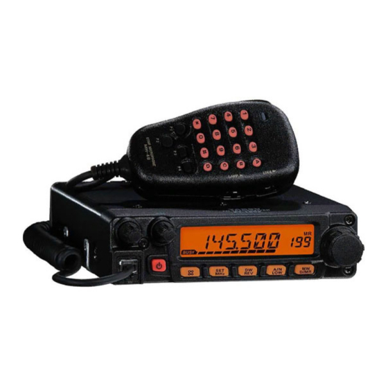
FT-1807M
Technical Supplement
©2006 VERTEX STANDARD CO., LTD.
Introduction
This manual provides technical information necessary for servicing the FT-1807M FM Transceiver.
Servicing this equipment requires expertise in handling surface-mount chip components. Attempts by non-
qualified persons to service this equipment may result in permanent damage not covered by the warranty,
and may be illegal in some countries.
Two PCB layout diagrams are provided for each double-sided circuit board in the Transceiver. Each side of is
referred to by the type of the majority of components installed on that side ("leaded" or "chip-only"). In most
cases one side has only chip components, and the other has either a mixture of both chip and leaded compo-
nents (trimmers, coils, electrolytic capacitors, ICs, etc.), or leaded components only.
While we believe the technical information in this manual to be correct, VERTEX STANDARD assumes no
liability for damage that may occur as a result of typographical or other errors that may be present. Your
cooperation in pointing out any inconsistencies in the technical information would be appreciated.
This transceiver was assembled using Pb (lead) free solder, based on the RoHS specification.
Only lead-free solder (Alloy Composition: Sn-3.0Ag-0.5Cu) should be used for repairs performed on
this apparatus. The solder stated above utilizes the alloy composition required for compliance with the
lead-free specification, and any solder with the above alloy composition may be used.
Specifications ...................................................... 2
Exploded View & Miscellaneous Parts ............ 3
Block Diagram .................................................... 5
Connection Diagram .......................................... 6
Circuit Description............................................. 7
Alignment ............................................................ 9
VERTEX STANDARD CO., LTD.
4-8-8 Nakameguro, Meguro-Ku, Tokyo 153-8644, Japan
VERTEX STANDARD
US Headquarters
10900 Walker Street, Cypress, CA 90630, U.S.A.
YAESU EUROPE B.V.
P.O. Box 75525, 1118 ZN Schiphol, The Netherlands
YAESU UK LTD.
Unit 12, Sun Valley Business Park, Winnall Close
Winchester, Hampshire, SO23 0LB, U.K.
VERTEX STANDARD HK LTD.
Unit 5, 20/F., Seaview Centre, 139-141 Hoi Bun Road,
Kwun Tong, Kowloon, Hong Kong
EH023U90A
Important Note
Contents
Board Unit
MAIN Unit Circuit Diagram ................................. 13
MAIN Unit Parts Layout ....................................... 15
MAIN Unit Parts List ............................................ 17
CNTL Unit Circuit Diagram .................................. 27
CNTL Parts Layout ............................................... 28
CNTL Parts List .................................................... 29
(Schematics, Layouts & Parts)
Advertisement
Table of Contents

Related Manuals for Yaesu FT-1807M


Summary of Contents for Yaesu FT-1807M
-
Page 1: Table Of Contents
(trimmers, coils, electrolytic capacitors, ICs, etc.), or leaded components only. While we believe the technical information in this manual to be correct, VERTEX STANDARD assumes no liability for damage that may occur as a result of typographical or other errors that may be present. Your cooperation in pointing out any inconsistencies in the technical information would be appreciated. -
Page 2: Specifications
Specifications General Frequency Range: Channel Step: Standard Repeater Shift: Frequency Stability: Modes of Emission: Antenna Impedance: Supply voltage: Current Consumption (typical): Operating Temperature Range: Case Size (WxHxD): Weight (Approx.): Transmitter Output Power: Modulation Type: Maximum Deviation: Spurious Radiation: Microphone Impedance: Receiver Circuit Type: Ifs:... -
Page 3: Exploded View & Miscellaneous Parts
DESCRIPTION MICROPHONE ( MH-48 AAA43X001 DC CABLE ( FT-1807M ) T9021715 DC CABLE ( FT-1807E ) T9022815 SPARE FUSE ( 15 A: FT-1807M ) Q0000081 SPARE FUSE ( 15 A: FT-1807E ) Q0000075 BRACKET ( MMB-36 ) D6000055 CB0297000 SCREW SET REF. - Page 4 Note...
-
Page 5: Block Diagram
Block Diagram... -
Page 6: Connection Diagram
Connection Diagram... -
Page 7: Circuit Description
Receive Signal Path Incoming RF signal is from the antenna jack is deliv- ered to the Main Unit and passed through the low- pass filter network consisting capacitors C1213, C1236, C1239, & C1238 and coils L1017, L1018, & L1019, antenna switching diode D1020 and D1028 (both RLS135), delivery to the RF amplifier Q1045 (3SK296ZQ). - Page 8 Circuit Description TX APC Circuit A portion of the power amplifier module output is rectified by D1022 (1SS321), then delivered to APC Q1038 (LM2904PWR), as a DC voltage which is pro- portional to the output level of the power amplifier module.
-
Page 9: Alignment
Introduction The FT-1807M is carefully aligned at the factory for the specified performance across the amateur band. Realignment should therefore not be necessary ex- cept in the event of a component failure. Only an authorized Vertex Standard representative should perform all component replacement and service, or the warranty policy may be void. -
Page 10: Test Setup
Deviation Meter Frequency Counter Entering the Alignment Mode Alignment of the FT-1807M is performed using a front panel software-based procedure. To perform alignment of the transceiver, it must first be placed in the “Alignment Mode,” in which the adjustments will be made and then stored into memory. - Page 11 Squelch Threshold Level Inject a 435.100 MHz signal at a level of –14 dBµ (with 1 kHz modulation @±3.5 kHz deviation) from the RF signal generator. Rotate the SQL knob to the 10-o’clock position. Rotate the DIAL knob to set the alignment param- 435.100 tL 435.100 tL.”...
- Page 12 Alignment CTCSS TX Deviation Rotate the DIAL knob to set the alignment param- eter to “435.000 103 435.000 103 435.000 103 435.000 103.” 435.000 103 Press the [ D/MR ( MW )] key to enable adjustment of the “CTCSS TX Deviation.” Press the PTT switch to activate the transmitter, adjust the DIAL knob so that the Deviation Meter reading is 0.6 kHz (±0.05 kHz).
-
Page 13: Main Unit Circuit Diagram
3.5 V (3.5 V) (0 V) 1.7 V 1.5 V (1.7 V) (1.5 V) (0.8 V) 1.0 V (1.0 V) 0.6 V (0.6 V) (0 V) 1.5 V (1.5 V) 3.8 V (3.8 V) 4.8 V 5.0 V (4.8 V) (5.0 V) 4.6 V 7.9 V... - Page 14 MAIN Unit Note...
-
Page 15: Main Unit Parts Layout
RA55H4047M KIA7808API LA4425A (Q1030) (Q1015) (Q1035) 2SA1774 (FR) 2SJ562 2SC4154 (E) (Q1007) (Q1008) (Q1033) 2SC4400 (RT4) (Q1032) 2SC4617 (BR) (Q1051, 1053) 2SC5226 (R22) (Q1026) 2SC4915O (Q0) CD4094BPWR 3SK296ZQ (ZQ) (Q1054) (Q1048) (Q1037, 1045) 2SC5374 (NA) MB15A01PFV1 (Q1009, 1010, 1017, (Q1011) 1023) NJM2591V (Q1028) -
Page 16: Main Unit
MAIN Unit Parts Layout (Side B) LM2902PWR LM2904PWR (Q1005, 1049) (Q1038, 1044, 1050) 2SA1774 (FR) 2SJ347 (KS) (Q1024, 2027, 1029) (Q1039) 2SC4154 (E) DTC144EE (26) S-812C50AUA (Q1001, 1021, 1046, (Q1013, 1020, 1022, 1047) 1031, 1040) FMMTL718TA (Q1025) DA221 (26) 1SS321 (F9) (D1009) (D1022) DAN222 (N) -
Page 17: Main Unit Parts List
GRM188B11H102KA01D GRM1882C1H101JA01D 6.3V JMK107BJ475MA-T GRM188B11H102KA01D GRM188B11H102KA01D GRM39B223K25PT GRM39B153K25PT GRM1882C1H151JA01D GRM39CH561J25PT GRM188B11H102KA01D MAIN Unit Parts List VXSTD P/N VERS. LOT SIDE LAY ADR CB3539001 FT-1807M CB3539002 FT-1807E FR014760C K78100072 K78100072 K22144802 K22174235 K22174809 K40129065 K22174265 K22174208 K22174803 K22174809 K22174809 K22174809 K22174809... -
Page 18: Parts List
MAIN Unit Parts List DESCRIPTION VALUE C 1082 AL.ELECTRO.CAP. 100uF C 1083 CHIP CAP. 0.001uF C 1084 CHIP CAP. 0.001uF C 1086 CHIP CAP. 0.01uF C 1087 CHIP CAP. 100pF C 1089 CHIP CAP. 0.1uF C 1090 CHIP CAP. 0.01uF C 1091 CHIP CAP. - Page 19 DESCRIPTION VALUE C 1166 CHIP CAP. 0.01uF C 1167 CHIP CAP. 100pF C 1168 CHIP CAP. 0.01uF C 1170 CHIP CAP. 10pF C 1171 CHIP CAP. C 1173 CHIP CAP. 0.1uF C 1174 CHIP CAP. 27pF C 1175 CHIP CAP. 0.01uF C 1176 CHIP CAP.
- Page 20 MAIN Unit Parts List DESCRIPTION VALUE C 1251 CHIP CAP. C 1252 CHIP CAP. C 1253 CHIP CAP. 0.001uF C 1254 CHIP CAP. 0.001uF C 1255 CHIP CAP. 0.01uF C 1256 CHIP CAP. 0.001uF C 1257 CHIP CAP. 0.01uF C 1258 CHIP CAP.
- Page 21 DESCRIPTION VALUE L 1003 CHIP COIL 0.0033uH L 1004 M.RFC 0.022uH L 1005 M.RFC 0.015uH L 1006 M.RFC 0.01uH L 1007 M.RFC 0.082uH L 1008 M.RFC 0.39uH L 1010 COIL 0.056uH L 1011 M.RFC 0.39uH L 1012 CHIP COIL 0.012uH L 1013 COIL 0.0068uH...
- Page 22 MAIN Unit Parts List DESCRIPTION VALUE R 1004 CHIP RES. R 1005 CHIP RES. R 1006 CHIP RES. R 1007 CHIP RES. 2.2k R 1008 CHIP RES. 2.2k R 1009 CHIP RES. 2.2k R 1010 CHIP RES. 1.5k R 1011 CHIP RES.
- Page 23 DESCRIPTION VALUE R 1092 CHIP RES. 2.2k R 1093 CHIP RES. R 1094 CHIP RES. R 1095 CHIP RES. R 1096 CHIP RES. R 1097 CHIP RES. R 1098 CHIP RES. R 1100 CHIP RES. R 1101 CHIP RES. R 1102 CHIP RES.
- Page 24 MAIN Unit Parts List DESCRIPTION VALUE R 1173 CHIP RES. R 1175 CHIP RES. R 1177 CHIP RES. R 1178 CHIP RES. 150k R 1179 CHIP RES. R 1180 CHIP RES. 470k R 1181 CHIP RES. 2.7k R 1182 CHIP RES. R 1183 CHIP RES.
- Page 25 DESCRIPTION VALUE R 1257 CHIP RES. 2.7k R 1258 CHIP RES. R 1259 CHIP RES. R 1260 CHIP RES. 470k TH1002 THERMISTOR TH1003 THERMISTOR X 1001 XTAL NX5032SA 11.7MHz XF1001 XTAL FILTER XF1002 XTAL FILTER SHIELD CASE SHIELD PLATE TOL. MFR'S DESIG 1/16W RMC1/16S 272JTH...
- Page 26 MAIN Unit Note...
-
Page 27: Cntl Unit Circuit Diagram
(0 V) (0 V) 5.0 V (5.0 V) (0 V) 4.8 V (0.6 V) 5.0 V (5.0 V) 4.8 V (0.6 V) 4.8 V (4.8 V) J2003 5.0 V 5.0 V 1.9 V 1.8 V 3.0 V 3.0 V 1.1 V 3.2 V 4.9 V 4.9 V... -
Page 28: Cntl Parts Layout
CNTL Unit Parts Layout CPH6202 (CB) (Q2005) (Side A) HD64F2266TF13 (Q2002) 2SC4617 (BR) (Q2007, 2008, 2013) 2SC5374 (NA) (Q2003) (Side B) S-812C50AUA (Q2010) DA221 (26) (D2001, 2025) DTC143ZE (E23) (Q2004) BR24L64 (Q2006) BD4830FVE (Q2011) DAN222 (N) (D2023) -
Page 29: Cntl Parts List
GRM188B11C104KA01D GRM155B11H102KA01D GRM155B11H102KA01D 6.3V GRM155B30J105KE18D GRM155B11H102KA01D DA221 TL CNTL Unit Parts List VXSTD P/N VERS. LOT SIDE LAY ADR CB3540001 FT-1807M A2 CB3540002 FT-1807M A1 CB3540003 FT-1807M A3 CB3540004 FT-1807E B1 CB3540005 FT-1807E B2 CB3540006 FT-1807M B3 CB3540007 FT-1807E C1... - Page 30 G3070102 G3070265 G1093876 G3346178R G3346178R G1093652 G1094121 G3346178R J24189053 J24189053 J24189013 J24189013 J24189013 J24189025 J24189025 J24189025 J24189013 J24189013 J24189013 J24189041 J24189049 J24189061 J24189043 J24189013 J24189013 J24189013 J24189041 J24189049 J24189025 J24189025 J24189384 J24189331 J24189374 J24189025 J24189049 : Please contact VERTEX STANDARD...
- Page 31 DESCRIPTION VALUE R 2031 CHIP RES. R 2032 CHIP RES. R 2033 CHIP RES. R 2034 CHIP RES. R 2036 CHIP RES. R 2037 CHIP RES. 220k R 2038 CHIP RES. 6.8k R 2039 CHIP RES. R 2040 CHIP RES. 220k R 2041 CHIP RES.
- Page 32 CNTL Unit Note...
- Page 34 Copyright 2006 VERTEX STANDARD CO., LTD. All rights reserved No portion of this manual may be reproduced without the permission of VERTEX STANDARD CO., LTD.