Sony CDP-CE275 Service Manual
Hide thumbs
Also See for CDP-CE275:
- Operating instructions manual (16 pages) ,
- Service manual (11 pages) ,
- Specifications (2 pages)
Table of Contents
Advertisement
Quick Links
CDP-CE275/CE375
SERVICE MANUAL
Ver 1.1 2001.07
Compact disc player
Semiconductor laser ( λ = 780 nm)
Laser
Emission duration : continuous
2 Hz to 20 kHz ± 0.5 dB
Frequency response
Dynamic range
More than 93 dB
Harmonic distortion
Less than 0.0045%
Outputs
Jack
type
ANALOG
Phono
OUT
jacks
DIGITAL
Optical
OUT
output
(OPTICAL)
connector
PHONES
Stereo
(CDP-CE375
phone
only)
jack
Sony Corporation
9-873-822-12
2001G0500-1
Home Audio Company
C 2001.7
Shinagawa Tec Service Manual Production Group
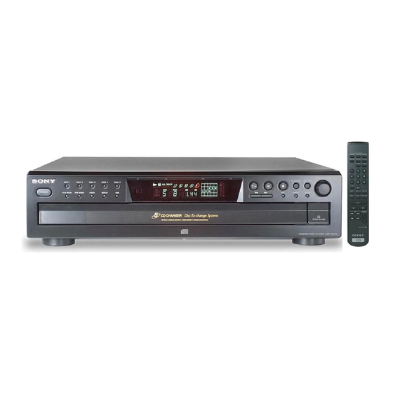
Photo: CDP-CE375
SPECIFICATIONS
Maximum
Load
output level
impedance
2 V
Over 10
(at 50 kilohms) kilohms
–18 dBm
Wave
length:
660 nm
10 mW
32 ohms
Model Name Using Similar Mechanism
CD Mechanism Type
Base Unit Name
Optical Pick-up Name
General
Power requirements
120 V AC, 60 Hz
Power consumption
11 W
Dimensions (approx.)
430 x 110 x 400 mm
(w/h/d)
(17 x 4 3/8 x 15 3/4 in.)
incl. projecting parts
Mass (approx.)
5 kg (11 lbs 1 oz)
Supplied accessories
Audio cord (2 phono plugs – 2 phono plugs) (1)
Remote commander (remote) (1) (CDP-CE375 only)
R6 (size AA) batteries (2) (CDP-CE375 only)
Design and specifications are subject to change without notice.
COMPACT DISC PLAYER
US Model
Canadian Model
Australian Model
CDP-CE275/CE375
AEP Model
UK Model
E Model
CDP-CE375
CDP-CE345
CDM59-5BD27
BU-5BD27
PXR-104X
Advertisement
Table of Contents

Related Manuals for Sony CDP-CE275


Summary of Contents for Sony CDP-CE275
- Page 1 CDP-CE275/CE375 SERVICE MANUAL US Model Canadian Model Ver 1.1 2001.07 Australian Model CDP-CE275/CE375 AEP Model UK Model E Model CDP-CE375 Photo: CDP-CE375 Model Name Using Similar Mechanism CDP-CE345 CD Mechanism Type CDM59-5BD27 Base Unit Name BU-5BD27 Optical Pick-up Name PXR-104X...
-
Page 2: Table Of Contents
SUR LES DIAGRAMMES SCHÉMATIQUES ET LA LISTE DES PIÈCES SONT CRITIQUES POUR LA SÉCURITÉ DE FONCTIONNEMENT. NE REMPLACER CES COM- POSANTS QUE PAR DES PIÈCES SONY DONT LES NUMÉROS SONT DONNÉS DANS CE MANUEL OU DANS LES SUPPLÉMENTS PUBLIÉS PAR SONY. -
Page 3: Servicing Notes
• Do not touch the soldering iron on the same conductor of the circuit board (within 3 times). • Be careful not to apply force on the conductor when soldering or unsoldering. Part No. Model Part No. CDP-CE275: US model 4-233-719-0s CDP-CE275: Canadian model 4-233-719-1s CDP-CE275: Australian model 4-233-719-2s CDP-CE375: US model... -
Page 4: General
CDP-CE275/CE375 SECTION 2 GENERAL • LOCATION OF CONTROLS – Front panel – 1 POWER button qs CLEAR button 2 DISC1 – DISC5 button qd CHECK button 3 Fluorescent indicator tube display qf EDIT button 4 H button qg M button... -
Page 5: Disassembly
CDP-CE275/CE375 SECTION 3 DISASSEMBLY • The equipment can be removed using the following procedure. Case Front Panel Assy CD Mechanism Block Base Unit (BU-5BD27) Optical Pick-up Tray, Table Assy Sensor Board Jnuction Board, Loading Motor Board Note: Follow the disassembly procedure in the numerical order given. - Page 6 CDP-CE275/CE375 3-2. FRONT PANEL ASSY 2 CN602 1 CN601 7 claw 3 CN301 8 front panel assy 4 CN351 6 claw 5 three screws (BVTP 3x8) 3-3. CD MECHANISM BLOCK (CDM59-5BD27) 6 two screws 4 two screws (BVTP 3x8) (BVTP 3x8)
- Page 7 CDP-CE275/CE375 3-4. BASE UNIT (BU-5BD27) 3 two screws (+PTPWHM 2.6), 2 two screws floating (+PTPWHM 2.6), floating 7 base unit (BU-5BD27) 6 spring (932), 5 spring (932), compression compression 4 holder (BU) assy 1 two screws (+PTPWHM 2.6), floating 3-5. TRAY, TABLE ASSY 8 screw (+PTPWHM 2.6), floating...
- Page 8 CDP-CE275/CE375 3-6. SENSOR BOARD 1 belt (rotary) table assy 4 SENSOR board 2 two screws (M 2.6), +BTTP 3 two screws (M 2.6), +BTTP 3-7. JUNCTION BOARD, LOADING MOTOR BOARD 6 two screws (M 2.6), +BTTP 4 JUNCTION board 2 CN13...
- Page 9 CDP-CE275/CE375 3-8. OPTICAL PICK-UP 4 connector 3 optical pick-up 2 shaft, sled...
-
Page 10: Test Mode
CDP-CE275/CE375 Ver 1.1 2001.07 SECTION 4 TEST MODE ADJ MODE Connecting Location: – MAIN BOARD (Component Side) – NOTE: This mode cannot be performed without a general remote com- mander. 1. Chuck the CD first, and then turn OFF the power. - Page 11 CDP-CE275/CE375 Ver 1.1 2001.07 All lit Buttons and Corresponding Button Numbers Button Button Number or Display ALL1DISCS PROGRAM DISC1 REPEAT 1 SHUFFLE 9 10 EDIT DISC TRACK PEAK STEP DISC2 TIME 11 12 13 14 15 FADE 16 17 18 19 20...
- Page 12 CDP-CE275/CE375 Ver 1.1 2001.07 AGING MODE For the aging mode, three modes of all mode, disc table mode, and loading mode are available. This set has the Aging mode for operation check of the mechanism deck. • If a failure occurred The aging operation stops and a faulty status is displayed on the fluorescent indicator tube.
-
Page 13: Electrical Adjustments
CDP-CE275/CE375 Ver 1.1 2001.07 SECTION 5 ELECTRICAL ADJUSTMENTS Procedure: Note: 1. CD Block is basically designed to operate without adjustment. There- Set the test disc (PATD-012). Disc chucking operation is fore, check each item in order given. [POWER] complete, then press the button to turn the power 2. - Page 14 CDP-CE275/CE375 Ver 1.1 2001.07 E-F Balance Check Checking Location: Connection: – BD BOARD (Conductor Side) – oscilloscope BD board TP (TE1) TP (VC) – Procedure: Set the test disc (PATD-012). Disc chucking operation is [POWER] complete, then press the button to turn the power off.
-
Page 15: Diagrams
CDP-CE275/CE375 SECTION 6 DIAGRAMS 6-1. NOTE FOR PRINTED WIRING BOARDS AND SCHEMATIC DIAGRAMS • Circuit Boards Location Note on Schematic Diagram: Note on Printed Wiring Board: • All capacitors are in µF unless otherwise noted. pF: µµF • X : parts extracted from the component side. -
Page 16: Printed Wiring Board - Bd Board
CDP-CE275/CE375 Ver 1.1 2001.07 6-2. PRINTED WIRING BOARD – BD Board – • See page 15 for Circuit Boards Location. (VC) (FE1) (TE1) (Page 20) TP (RFDC) TP (RFAC) • Semiconductor • Semiconductor Location Location Ref. No. Location Ref. No. Location... -
Page 17: Schematic Diagram - Bd Board
CDP-CE275/CE375 Ver 1.1 2001.07 6-3. SCHEMATIC DIAGRAM – BD Board – • • See page 24 for Waveforms. See page 24 for IC Block Diagrams. (RFAC) IC BD (RFDC) (TE1) (VC) (FE1) (SE1) IC BD (Page 21) The components identified by mark 0 or dotted Les composants identifiés par une marque 0 sont... -
Page 18: Printed Wiring Boards - Junction/Sensor/ Loading Motor Boards
CDP-CE275/CE375 6-4. PRINTED WIRING BOARDS – JUNCTION/SENSOR/LOADING MOTOR Boards – • See page 15 for Circuit Boards Location. (Page 20) TO MAIN BOARD • Semiconductor Location Ref. No. Location IC11 • Semiconductor Location Ref. No. Location... -
Page 19: Schematic Diagram - Junction/Sensor/ Loading Motor Boards
CDP-CE275/CE375 6-5. SCHEMATIC DIAGRAM – JUNCTION/SENSOR/LOADING MOTOR Boards – • See page 25 for IC Block Diagram. TO MAIN BOARD (Page 21) IC BD... -
Page 20: Printed Wiring Board - Main Board
CDP-CE275/CE375 Ver 1.1 2001.07 6-6. PRINTED WIRING BOARD – MAIN Board – • See page 15 for Circuit Boards Location. (Page 22) (Page 22) TP1 (ADJ) TP2 (AFDJ) (Page 22) • Semiconductor Location Ref. No. Location Ref. No. Location (Page 18) -
Page 21: Schematic Diagram - Main Board
CDP-CE275/CE375 6-7. SCHEMATIC DIAGRAM – MAIN Board – • See page 24 for Waveform. (Page 23) (Page 17) (Page 23) (Page 23) (Page 19) The components identified by mark 0 or dotted Les composants identifiés par une marque 0 sont line with mark 0 are critical for safety. -
Page 22: Printed Wiring Boards - Panel Section
CDP-CE275/CE375 6-8. PRINTED WIRING BOARDS – PANEL Section – • See page 15 for Circuit Boards Location. (Page 20) • Semiconductor Location Ref. No. Location IC802 A-13 (Page 20) (Page 20) -
Page 23: Schematic Diagram - Panel Section
CDP-CE275/CE375 6-9. SCHEMATIC DIAGRAM – PANEL Section – (Page 21) (Page 21) (Page 21) The components identified by mark 0 or dotted Les composants identifiés par une marque 0 sont line with mark 0 are critical for safety. critiques pour la sécurité. Ne les remplacer que Replace only with part number specified. - Page 24 CDP-CE275/CE375 • Waveforms • IC Block Diagrams – BD Board – – MAIN Board – – BD BOARD – IC101 CXD2587Q 1 IC101 yj (XTAO) 5 IC101 el (FE) (CD Play Mode) 1 IC301 es (XTAL) 4.2 Vp-p 3.1 Vp-p 0.5 Vp-p...
- Page 25 CDP-CE275/CE375 – BD Board – IC131 CXA2581N DC_OFST RW/ROM RFDCI DVCC 11 RFDCO EQ IN 26 RFC 25 VFC 24 BST AC SUM ON/OFF 23 RFG VOFST 22 VCC RW/ROM VOFST RW/ROM RW/ROM 19 TE_BAL DVCC RW/ROM 18 TE APC-OFF(Hi-Z)
-
Page 26: 6-10. Ic Pin Function Description
CDP-CE275/CE375 6-10. IC PIN FUNCTION DESCRIPTION • BD BOARD IC101 CXD2587Q (DIGITAL SIGNAL PROCESSOR, DIGITAL SERVO PROCESSOR, DIGITAL FILTER, D/A CONVERTER) Pin No. Pin Name Description SQSO Subcode Q data output to the system controller (IC301) SQCK Subcode Q data reading clock signal input from the system controller (IC301) XRST System reset signal input from the system controller (IC301) “L”: reset... - Page 27 CDP-CE275/CE375 Pin No. Pin Name Description RFDC RF signal input from the CXA2568M (IC103) ADIO Monitor output of the A/D converter input signal Not used (open) AVSS0 — Ground terminal (digital system) IGEN Stabilized current input for operational amplifiers AVDD0 —...
- Page 28 CDP-CE275/CE375 • MAIN BOARD IC301 CXP82532-013Q (SYSTEM CONTROLLER, FLUORESCENT INDICATOR TUBE DRIVER, KEY CONTROL) Pin No. Pin Name Description BUSIN Sircs remote control signal input terminal Not used (pull up) RMIN Remote control signal input from the remote control receiver (IC802)
- Page 29 CDP-CE275/CE375 Pin No. Pin Name Description 38 to 57 P1 to P20 Segment drive signal output to the fluorescent indicator tube (FL801) 58 to 62 Not used (open) 63 to 70 G1 to G8 Grid drive signal output to the fluorescent indicator tube (FL801) —...
-
Page 30: Exploded Views
CDP-CE275/CE375 SECTION 7 EXPLODED VIEWS NOTE: • -XX and -X mean standardized parts, so they • Items marked “*” are not stocked since they The components identified by mark 0 or dotted line with mark may have some difference from the original are seldom required for routine service. -
Page 31: Front Panel Section
CDP-CE275/CE375 7-2. FRONT PANEL SECTION FL801 not supplied supplied with J881 Ref. No. Part No. Description Remark Ref. No. Part No. Description Remark A-4953-509-1 PANEL ASSY, FRONT (CE375:US/CND) 4-231-973-11 BUTTON (POWER)(CE375:AEP) X-4953-510-1 PANEL ASSY, FRONT(SILVER)(CE375:AEP) 1-681-141-21 POWER SW BOARD X-4953-511-1 PANEL ASSY, FRONT(BLACK)(CE275:US/CND) - Page 32 CDP-CE275/CE375 7-3. CD MECHANISM SECTION (1) (CDM59-5BD27) not supplied not supplied BU-5BD27 not supplied not supplied Ref. No. Part No. Description Remark Ref. No. Part No. Description Remark 4-224-619-01 BRACKET (GUIDE) 1-791-930-11 WIRE (FLAT TYPE)(6 CORE) 4-218-253-31 SCREW (M2.6), +BTTP...
- Page 33 CDP-CE275/CE375 7-4. CD MECHANISM SECTION (2) (CDM59-5BD27) not supplied not supplied Ref. No. Part No. Description Remark Ref. No. Part No. Description Remark X-4952-019-2 PULLEY (A) ASSY, CHUCKING 4-224-607-01 GEAR, SWING 1-676-246-11 JUNCTION BOARD 4-224-609-01 GEAR (LOADING C) 4-218-253-31 SCREW (M2.6), +BTTP...
- Page 34 CDP-CE275/CE375 7-5. BASE UNIT SECTION (BU-5BD27) M101 M102 The components identified by Les composants identifiés par une mark 0 or dotted line with marque 0 sont critiques pour la mark 0 are critical for safety. sécurité. Replace only with part num- Ne les remplacer que par une pièce...
-
Page 35: Electrical Parts List
CDP-CE275/CE375 SECTION 8 ELECTRICAL PARTS LIST NOTE: • Due to standardization, replacements in the • Items marked “*” are not stocked since they The components identified by mark 0 or dotted line with mark parts list may be different from the parts speci- are seldom required for routine service. -
Page 36: Disc1
CDP-CE275/CE375 DISPLAY Ref. No. Part No. Description Remark Ref. No. Part No. Description Remark R138 1-216-798-11 RES-CHIP 1/16W < RESISTOR > R139 1-216-847-11 METAL CHIP 150K 1/16W R811 1-249-415-11 CARBON 1/4W F R140 1-216-854-11 METAL CHIP 560K 1/16W R812 1-249-417-11 CARBON... -
Page 37: Play Mode
CDP-CE275/CE375 MAIN Ref. No. Part No. Description Remark Ref. No. Part No. Description Remark 1-681-140-11 KEY BOARD (CE275,CE375:US/CND) A-4725-570-A MAIN BOARD, COMPLETE (CE275) ***************************** ********************* 1-681-140-21 KEY BOARD (CE375:AUS/AEP/UK/SP/E) A-4725-571-A MAIN BOARD, COMPLETE (CE375:US/CND) ******************************** ********************* < CAPACITOR > A-4725-579-A MAIN BOARD, COMPLETE... - Page 38 CDP-CE275/CE375 MAIN Ref. No. Part No. Description Remark Ref. No. Part No. Description Remark D605 8-719-024-99 DIODE 11ES2-NTA2B R352 1-249-441-11 CARBON 100K 1/4W D606 8-719-110-08 DIODE RD8.2ESB2 R353 1-249-441-11 CARBON 100K 1/4W D607 8-719-991-33 DIODE 1SS133T-77 D608 8-719-109-85 DIODE RD5.1ESB2...
- Page 39 CDP-CE275/CE375 SENSOR JUNCTION POWER SW LOADING MOTOR Ref. No. Part No. Description Remark Ref. No. Part No. Description Remark 1-681-141-11 POWER SW BOARD (CE275,CE375:US/CND) < SWITCH > **************** 1-771-836-11 SWITCH, LEVER (SLIDE) 1-681-141-21 POWER SW BOARD ************************************************************** (CE375:AUS/AEP/UK/SP/E) MISCELLANEOUS **************** *************** <...
- Page 40 CDP-CE275/CE375 REVISION HISTORY Clicking the version allows you to jump to the revised page. Also, clicking the version at the upper right on the revised page allows you to jump to the next revised page. Ver. Date Description of Revision 2001.07...