Table of Contents
Advertisement
CDX-R3350/R3350C
QQ
3 7 63 1515 0
SERVICE MANUAL
Ver. 1.0 2004.12
• The tuner and CD sections have no adjustments.
TE
CD player section
L 13942296513
Signal-to-noise ratio
120 dB
Frequency response
10 – 20,000 Hz
Wow and flutter
Below measurable limit
Tuner section
FM
Tuning range
87.5 – 108 MHz
Antenna terminal
External antenna connector
Intermediate frequency 10.7 MHz/450 kHz
Usable sensitivity
9 dBf
Selectivity
75 dB at 400 kHz
Signal-to-noise ratio
67 dB (stereo),
69 dB (mono)
Harmonic distortion at 1 kHz
0.5% (stereo),
0.3% (mono)
Separation
35 dB at 1 kHz
Frequency response
30 – 15,000 Hz
www
.
Sony Corporation
9-879-385-01
2004L04-1
e Vehicle Company
© 2004. 12
Published by Sony Engineering Corporation
http://www.xiaoyu163.com
x
ao
u163
y
i
http://www.xiaoyu163.com
2 9
8
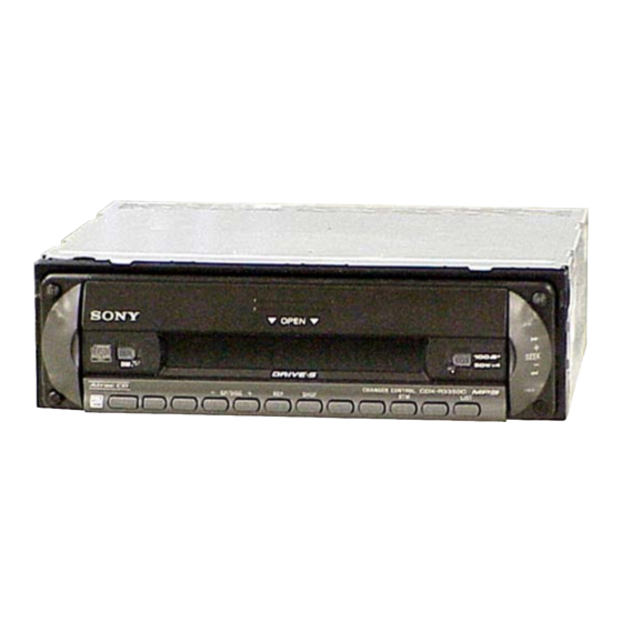
Photo: CDX-R3350C
Model Name Using Similar Mechanism
CD Drive Mechanism Type
Optical Pick-up Name
SPECIFICATIONS
Q Q
3
6 7
1 3
1 5
MW/LW
Tuning range
Antenna terminal
Intermediate frequency 10.7 MHz/450 kHz
Sensitivity
Power amplifier section
Outputs
Speaker impedance
Maximum power output 50 W × 4 (at 4 ohms)
General
Outputs
Inputs
FM/MW/LW COMPACT DISC PLAYER
co
.
9 4
2 8
AEP Model
UK Model
NEW
MG-611TA-186//Q
KSS1000E
0 5
8
2 9
9 4
2 8
MW: 531 – 1,602 kHz
LW: 153 – 279 kHz
External antenna connector
MW: 30 µV
LW: 40 µV
Speaker outputs
(sure seal connectors)
4 – 8 ohms
Audio outputs terminal
(front (CDX-R3350C only), sub/rear switchable)
Power antenna relay control terminal
Power amplifier control terminal
Telephone ATT control terminal
BUS control input terminal (CDX-R3350C only)
BUS audio input terminal (CDX-R3350C only)
Remote controller input terminal
Antenna input terminal
– Continued on next page –
m
9 9
9 9
1
Advertisement
Table of Contents

Related Manuals for Sony CDX-R3350


Summary of Contents for Sony CDX-R3350
- Page 1 BUS audio input terminal (CDX-R3350C only) Remote controller input terminal Antenna input terminal – Continued on next page – FM/MW/LW COMPACT DISC PLAYER u163 Sony Corporation 9-879-385-01 2004L04-1 e Vehicle Company © 2004. 12 Published by Sony Engineering Corporation http://www.xiaoyu163.com...
- Page 2 Card remote commander RM-X151 US and foreign patents licensed from Dolby Laboratories. optical pick-up Note This unit cannot be connected to a digital preamplifier or an equalizer which is Sony BUS system compatible. Design and specifications are subject to change without notice.
- Page 3 CDX-R3350/R3350C 3 7 63 1515 0 • CD Playback: UNLEADED SOLDER You can play CD-DA (also containing CD TEXT* ), CD-R/CD- Boards requiring use of unleaded solder are printed with the lead RW (MP3 files also containing Multi Session and ATRAC CD free mark (LF) indicating the solder contains no lead.
-
Page 4: Table Of Contents
CDX-R3350/R3350C 3 7 63 1515 0 TABLE OF CONTENTS 1. GENERAL Location of Controls ..............5 Connections ................5 2. DISASSEMBLY 2-1. Sub Panel Assy (CD) ............8 2-2. CD Mechanism Block ............8 2-3. Main Board ................. 9 2-4. -
Page 5: General
CDX-R3350/R3350C SECTION 1 GENERAL 3 7 63 1515 0 This section is extracted from instruction manual. • LOCATION OF CONTROL o SENS/BTM button 8 Refer to the pages listed for details. The Location of controls and basic operations corresponding buttons on the card remote... - Page 6 CDX-R3350/R3350C 3 7 63 1515 0 Supplied with XA-C30 Note for the aerial connecting Remarque sur le raccordement de Opmerking bij de antenne-aansluiting Mit dem XA-C30 geliefert If your car aerial is an ISO (International l’antenne Indien uw auto is uitgerust met een...
-
Page 7: Disassembly
CDX-R3350/R3350C SECTION 2 DISASSEMBLY 3 7 63 1515 0 Note : This set can be disassemble according to the following sequence. 2-1. SUB PANEL ASSY (Page 8) 2-2. CD MECHANISM BLOCK (Page 8) 2-10. SERVO BOARD 2-4. CHASSIS (T) SUB ASSY 2-3. -
Page 8: Sub Panel Assy (Cd)
CDX-R3350/R3350C 3 7 63 1515 0 Note : Follow the disassembly procedure in the numerical order given. 2-1. SUB PANEL ASSY (CD) 3 two claws 2 two claws 1 two screws (+PTT 2.6 x 6) 4 sub panel assy L 13942296513 2-2. -
Page 9: Main Board
CDX-R3350/R3350C 3 7 63 1515 0 2-3. MAIN BOARD 1 three screws (+BTT 2.6 x 5) 2 two screws (+PTT 2.6 x 8) 3 MAIN board 4 insulating sheet L 13942296513 2-4. CHASSIS (T) SUB ASSY 4 claw 2 two screws (+P 1.7 x 2.2) -
Page 10: Roller Arm Assy
CDX-R3350/R3350C 3 7 63 1515 0 2-5. ROLLER ARM ASSY 3 washer 5 roller arm assy 4 gear (RA1) 2 spring (RAR) 1 spring (RAL) L 13942296513 2-6. CHASSIS (OP) ASSY qa chassis (OP) assy 0 coil spring (damper) -
Page 11: Optical Pick-Up
CDX-R3350/R3350C 3 7 63 1515 0 2-7. OPTICAL PICK-UP 2 chucking arm sub assy 5 claw 1 tension coil spring (CHKG) 7 optical pick-up 6 main shaft 4 rack (SL) 3 screw (+B 1.4 x 5) L 13942296513 2-8. SL MOTOR ASSY (M902) 1 screw (+P 1.4 x 1.8) -
Page 12: Le Motor Assy (M903)
CDX-R3350/R3350C 3 7 63 1515 0 2-9. LE MOTOR ASSY (M903) 8 screw 0 gear (LE) assy (+M 1.7 x 2.5) 9 bearing (LEB-N) 2 washer qa screw (+M 1.7 x 2.5) qf two toothed lock screws 3 gear (LE1) (+M 1.4 ) -
Page 13: Diagrams
CDX-R3350/R3350C SECTION 3 DIAGRAMS 3 7 6 3 1 5 1 5 0 3-1. BLOCK DIAGRAM — CD SECTION — • R-ch is omitted due to same as L-ch. • Signal Path : CD PLAY DETECTOR MAIN FPI2 CD-L... -
Page 14: Block Diagram -Main Section
CDX-R3350/R3350C 3 7 6 3 1 5 1 5 0 3-2. BLOCK DIAGRAM — MAIN SECTION — ELECTRONIC VOLUME R3350C IC401 BUS LCH AUDIO IN BUS RCH R-CH AUX IN R-CH CD-L 9 CD LCH SECTION OUT SUB L... -
Page 15: Block Diagram -Display Section
CDX-R3350/R3350C 3 7 6 3 1 5 1 5 0 3-3. BLOCK DIAGRAM — DISPLAY SECTION — 3-4. CIRCUIT BOARDS LOCATION SYSTEM CONTROL LCD DRIVER IC501 (3/3) IC901 SERVO board KEY MATRIX KEYIN0 SENSOR board LCDSO DATA S900-908, 910-922... - Page 16 CDX-R3350/R3350C 3 7 6 3 1 5 1 5 0 • WAVEFORMS • NOTE FOR PRINTED WIRING BOARDS AND SCHEMATIC DIAGRAMS THIS NOTE IS COMMON FOR PRINTED WIRING — SERVO BOARD — BOARDS AND SCHEMATIC DIAGRAMS. (CD PLAY) (In addition to this, the necessary note is printed in each block.)
-
Page 17: Printed Wiring Boards -Cd Mechanism Section
CDX-R3350/R3350C 3 7 6 3 1 5 1 5 0 3-5. PRINTED WIRING BOARDS — CD MECHANISM SECTION — • Refer to page 15 for Circuit Boards Location. : Uses unleaded solder. 1 3 9 4 2 2 9 6 5 1 3 1-689-230- •... -
Page 18: Schematic Diagram -Cd Mechanism Section (1/2)
CDX-R3350/R3350C 3 7 6 3 1 5 1 5 0 • Refer to page 16 for Waveforms. 3-6. SCHEMATIC DIAGRAM — CD MECHANISM SECTION (1/2) — • Refer to page 26 for IC Block Diagrams. IC B/D C102 TP25... -
Page 19: Schematic Diagram -Cd Mechanism Section (2/2)
CDX-R3350/R3350C 3 7 6 3 1 5 1 5 0 • Refer to page 16 for Waveform. • Refer to page 26 for IC Block Diagram. 3-7. SCHEMATIC DIAGRAM — CD MECHANISM SECTION (2/2) — • Refer to page 29 for IC Pin Description. -
Page 20: Printed Wiring Board -Main Section
CDX-R3350/R3350C 3-8. PRINTED WIRING BOARD — MAIN SECTION — • Refer to page 15 for Circuit Boards Location. : Uses unleaded solder. 3 7 6 3 1 5 1 5 0 R3350C R3350C R3350C CN601 JC12 CN580 C484 C474... -
Page 21: Schematic Diagram -Main Section (1/3)
CDX-R3350/R3350C 3 7 6 3 1 5 1 5 0 • Refer to page 16 for Waveform. 3-9. SCHEMATIC DIAGRAM — MAIN SECTION (1/3) — • Refer to page 26 for IC Block Diagrams. J330 C330 C331 C484 C474... -
Page 22: Schematic Diagram -Main Section (2/3)
CDX-R3350/R3350C 3 7 6 3 1 5 1 5 0 3-10. SCHEMATIC DIAGRAM — MAIN SECTION (2/3) — • Refer to page 28 for IC Block Diagram. C775 C765 C764 C774 C776 C751 D751 C752 D752 C750 D753 IC B/D... -
Page 23: Schematic Diagram -Main Section (3/3)
CDX-R3350/R3350C 3 7 6 3 1 5 1 5 0 • Refer to page 16 for Waveforms. • Refer to page 27 for IC Block Diagram. 3-11. SCHEMATIC DIAGRAM — MAIN SECTION (3/3) — • Refer to page 31 for IC Pin Description. -
Page 24: Printed Wiring Board -Display Section
CDX-R3350/R3350C 3 7 6 3 1 5 1 5 0 3-12. PRINTED WIRING BOARD — DISPLAY SECTION — • Refer to page 15 for Circuit Boards Location. : Uses unleaded solder. LED902 LED905 S906 S911 LED905, S905 R3350C S905... -
Page 25: Schematic Diagram -Display Section
CDX-R3350/R3350C 3 7 6 3 1 5 1 5 0 3-13. SCHEMATIC DIAGRAM — DISPLAY SECTION — R972 IC971 R987 LED910 LED913 LED917 LED921 LED922 R924 LED931 R988 C971 CN901 R989 R941 R925 R976 LED912 LED914 LED918 LED908 LED904... - Page 26 CDX-R3350/R3350C 3 7 6 3 1 5 1 5 0 • IC BLOCK DIAGRAMS IC2 TC94A60MFG-301 (SERVO Board (1/2)) IC1 BA5968FP-E2 (SERVO Board (2/2)) 72 71 66 65 64 63 62 61 60 59 58 56 55 54 53...
- Page 27 CDX-R3350/R3350C 3 7 63 1515 0 IC401 BD3806FS-FE2 (MAIN Board (1/3)) FADER FADER FADER FADER (0~-58, (0~-58, (0~-58, (0~-58, C BUS -∞dB) -∞dB) -∞dB) -∞dB) GAIN+ATT LOGIC (+10~-29, -∞dB) 2ND ORDER LPF EFFECT (0dB~ EFFECT (0dB~ fc:OFF,80,120,160Hz +20dB,2dB STEP)
- Page 28 CDX-R3350/R3350C 3 7 63 1515 0 IC750 TDA8588AJ/N2/R1 (MAIN Board (2/3)) (R3350C) IC750 TDA8588BJ/N2/R1 (MAIN Board (2/3)) (R3350) OUT FL- I2C BUS OUT FL+ OUT RL- PGND3 OUT RL+ INRL INFL SGND PROTECTION DIAGNOSTIC INFR INRR AC GND OUT RR+...
- Page 29 CDX-R3350/R3350C 3 7 63 1515 0 • IC PIN DESCRIPTIONS • IC3 MB90487APFV-G-142-BNDE1 (CD SYSTEM CONTROL) (SERVO BOARD (2/2)) Pin No. Pin Name Pin Description Servo 1.5 V power supply control signal output 2 to 6 — Not used. (Open)
- Page 30 CDX-R3350/R3350C 3 7 63 1515 0 Pin No. Pin Name Pin Description XUART Sony-Bus/MC-Bus change signal input H: Sony-Bus, L: MC-Bus ZMUTE Zero detection mute signal output MECON CHK MECON rising detection signal input CDON CHK CDON rising detection signal input 69 to 74 —...
- Page 31 BUIN Backup power supply detection signal input u163 CD INTQ Not used in this set. (Open) DAVN RDS data block synchronization detection signal input Not used. (Open) UNISI SONY BUS data signal input UNISO SONY BUS data signal output http://www.xiaoyu163.com...
- Page 32 CDX-R3350/R3350C 3 7 63 1515 0 Pin No. Pin Name Pin Description UNISCK SONY BUS clock signal output 61 to 63 Not used. (Open) SIRCS Remote control signal (infrared rays) input 65 to 67 Not used. (Open) Memory mode change signal input FLASH W Normally “H”...
-
Page 33: Exploded Views
CDX-R3350/R3350C SECTION 4 EXPLODED VIEWS 3 7 63 1515 0 NOTE: • The mechanical parts with no reference • Color Indication of Appearance Parts The components identified by mark 0 or dotted line with mark number in the exploded views are not supplied. -
Page 34: Front Panel Section
CDX-R3350/R3350C 3 7 63 1515 0 4-2. FRONT PANEL SECTION not supplied (KEY board) not supplied LCD901 not supplied not supplied not supplied not supplied supplied L 13942296513 not supplied not supplied Ref. No. Part No. Description Remark Ref. No. -
Page 35: Cd Mechanism Section (1)
CDX-R3350/R3350C 3 7 63 1515 0 4-3. CD MECHANISM SECTION (1) (MG-611TA-186//Q) not supplied (SENSOR board) not supplied not supplied L 13942296513 Ref. No. Part No. Description Remark Ref. No. Part No. Description Remark A-3372-444-A CHASSIS (T) SUB ASSY 3-352-758-31 SCREW (M1.7), TOOTHED LOCK... -
Page 36: Cd Mechanism Section (2)
CDX-R3350/R3350C 3 7 63 1515 0 4-4. CD MECHANISM SECTION (2) (MG-611TA-186//Q) (including M901) M902 not supplied not supplied L 13942296513 not supplied not supplied not supplied The components identified by mark 0 or dotted line with mark 0 are critical for safety. -
Page 37: Cd Mechanism Section (3)
CDX-R3350/R3350C 3 7 63 1515 0 4-5. CD MECHANISM SECTION (3) (MG-611TA-186//Q) M903 L 13942296513 Ref. No. Part No. Description Remark Ref. No. Part No. Description Remark 3-348-993-01 WASHER 2-186-696-01 BRACKET (LEM-N) 2-186-699-01 GEAR (RA1) 3-345-648-91 SCREW (M1.4), TOOTHED LOCK... -
Page 38: Cd Mechanism Section (4)
CDX-R3350/R3350C 3 7 63 1515 0 4-6. CD MECHANISM SECTION (4) (MG-611TA-186//Q) L 13942296513 Ref. No. Part No. Description Remark Ref. No. Part No. Description Remark 2-186-700-01 GEAR (CHK1) 3-899-829-01 WASHER (SLIT) 3-344-223-01 WASHER 3-259-032-01 GEAR (LE2) 3-259-470-11 GEAR (LE1) -
Page 39: Electrical Parts List
CDX-R3350/R3350C SECTION 5 ELECTRICAL PARTS LIST 3 7 63 1515 0 NOTE: • Due to standardization, replacements in • Items marked “*” are not stocked since The components identified by mark 0 or dotted line with mark the parts list may be different from the they are seldom required for routine service. - Page 40 CDX-R3350/R3350C MAIN 3 7 63 1515 0 Ref. No. Part No. Description Remark Ref. No. Part No. Description Remark Q903 6-551-244-01 TRANSISTOR MUN2233T1G (R3350C) R953 1-216-864-11 SHORT CHIP 0 (R3350) R961 1-216-817-11 METAL CHIP 1/10W < RESISTOR > R962...
- Page 41 CDX-R3350/R3350C MAIN 3 7 63 1515 0 Ref. No. Part No. Description Remark Ref. No. Part No. Description Remark 1-126-963-11 ELECT 4.7uF C501 1-162-970-11 CERAMIC CHIP 0.01uF 1-126-947-11 ELECT 47uF C502 1-162-964-11 CERAMIC CHIP 0.001uF 1-126-947-11 ELECT 47uF C503...
- Page 42 CDX-R3350/R3350C MAIN 3 7 63 1515 0 Ref. No. Part No. Description Remark Ref. No. Part No. Description Remark < CONNECTOR > FB603 1-216-295-11 SHORT CHIP FB604 1-216-295-11 SHORT CHIP CN580 1-580-907-41 PLUG, CONNECTOR (BUS CONTROL IN) FB605 1-216-864-11 SHORT CHIP...
- Page 43 CDX-R3350/R3350C MAIN 3 7 63 1515 0 Ref. No. Part No. Description Remark Ref. No. Part No. Description Remark Q441 6-551-070-01 TRANSISTOR KRC283S-B-RPK/P R431 1-216-809-11 METAL CHIP 1/10W Q451 6-551-070-01 TRANSISTOR KRC283S-B-RPK/P R432 1-216-841-11 METAL CHIP 1/10W Q461 6-551-070-01 TRANSISTOR KRC283S-B-RPK/P...
- Page 44 CDX-R3350/R3350C MAIN SENSOR SERVO 3 7 63 1515 0 Ref. No. Part No. Description Remark Ref. No. Part No. Description Remark R548 1-216-845-11 METAL CHIP 100K 1/10W R676 1-216-821-11 METAL CHIP 1/10W (R3350C) R677 1-216-821-11 METAL CHIP 1/10W R550...
- Page 45 CDX-R3350/R3350C SERVO 3 7 63 1515 0 Ref. No. Part No. Description Remark Ref. No. Part No. Description Remark 1-162-923-11 CERAMIC CHIP 47PF 1-208-699-11 METAL CHIP 4.7K 0.5% 1/16W 1-164-677-11 CERAMIC CHIP 0.033uF 1-208-912-11 METAL CHIP 0.5% 1/16W 1-125-777-11 CERAMIC CHIP 0.1uF...
- Page 46 CDX-R3350/R3350C SERVO 3 7 63 1515 0 Ref. No. Part No. Description Remark Ref. No. Part No. Description Remark 1-218-941-81 RES-CHIP 1/16W PARTS FOR INSTALLATION AND CONNECTIONS 1-218-941-81 RES-CHIP 1/16W *************************************** 1-218-973-11 RES-CHIP 1/16W 1-218-973-11 RES-CHIP 1/16W X-3382-647-1 FRAME ASSY, FITTING...
- Page 47 CDX-R3350/R3350C 3 7 63 1515 0 MEMO L 13942296513 u163 http://www.xiaoyu163.com...
- Page 48 CDX-R3350/R3350C 3 7 63 1515 0 REVISION HISTORY Clicking the version allows you to jump to the revised page. Also, clicking the version at the upper on the revised page allows you to jump to the next revised page.