Panasonic DMR-ES10EB Service Manual
Hide thumbs
Also See for DMR-ES10EB:
- Quick setup manual (6 pages) ,
- Operating instructions manual (48 pages) ,
- Service manual (71 pages)
Table of Contents
Advertisement
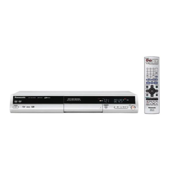
DVD Video Recorder
DMR-ES10EB
DMR-ES10EC
DMR-ES10EG
DMR-ES10EP
DMR-ES10EBL
Vol.1
Colour
(S).......... .............S ilver Type
(K).......... .............B lack Type
© 2005 Matsushita Electric Industrial CO., Ltd. All
rights
reserved.
distribution is a violation of law.
ORDER NO.DSD0503039C2
Unauthorized
copying
and
Advertisement
Table of Contents

Related Manuals for Panasonic DMR-ES10EB


Summary of Contents for Panasonic DMR-ES10EB
- Page 1 ORDER NO.DSD0503039C2 DVD Video Recorder DMR-ES10EB DMR-ES10EC DMR-ES10EG DMR-ES10EP DMR-ES10EBL Vol.1 Colour (S).......S ilver Type (K).......B lack Type © 2005 Matsushita Electric Industrial CO., Ltd. All rights reserved. Unauthorized copying distribution is a violation of law.
- Page 2 DMR-ES10EB / DMR-ES1 0EC / DMR-ES1 0EG / DMR-ES1 0EP / DMR-ES10EBL...
- Page 3 DMR-ES10EB / DMR-ES1 0EC / DMR-ES1 0EG / DMR-ES1 0EP / DMR-ES10EBL...
-
Page 4: Table Of Contents
DMR-ES10EB / DMR-ES1 0EC / DMR-ES1 0EG / DMR-ES1 0EP / DMR-ES10EBL CONTENTS Page Page 1 Safety precautions 13 Caution after replacing parts 1.1. General guidelines 13.1. After replacing the RAM Drive with new one 2 Prevention of Electrostatic Discharge (ESD) to Electrostatic 13.2. -
Page 5: Safety Precautions
DMR-ES10EB / DMR-ES1 0EC / DMR-ES1 0EG / DMR-ES1 0EP / DMR-ES10EBL 1 Safety precautions 1.1. General guidelines 1. When servicing, observe the original lead dress. If a short circuit is found, replace all parts which have been overheated or damaged by the short circuit. -
Page 6: Prevention Of Electrostatic Discharge (Esd) To Electrostatic Sensitive (Es) Devices
DMR-ES10EB / DMR-ES1 0EC / DMR-ES1 0EG / DMR-ES1 0EP / DMR-ES10EBL 2 Prevention of Electrostatic Discharge (ESD) to Electrostatic Sensitive (ES) Devices Some semiconductor (solid state) devices can be damaged easily by static electricity. Such components commonly are called Electrostatic Sensitive (ES) Devices. -
Page 7: Precaution Of Laser Diode
DMR-ES10EB / DMR-ES1 0EC / DMR-ES1 0EG / DMR-ES1 0EP / DMR-ES10EBL 3 Precaution of Laser Diode 4 Handling the Lead-free Solder 4.1. About lead free solder (PbF) Distinction of PbF P.C.B.: P.C.B.s (manufactured) using lead free solder will have a PbF stamp on the P.C.B. -
Page 8: Each Button
DMR-ES10EB / DMR-ES1 0EC / DMR-ES1 0EG / DMR-ES1 0EP / DMR-ES10EBL 5 Each Button For DMR-ES10EC/EG/EP... - Page 9 DMR-ES10EB / DMR-ES1 0EC / DMR-ES1 0EG / DMR-ES1 0EP / DMR-ES10EBL For DMR-ES10EB/EBL...
-
Page 10: New Feature
DMR-ES10EB / DMR-ES1 0EC / DMR-ES1 0EG / DMR-ES1 0EP / DMR-ES10EBL 6 New Feature 6.1. Quick start function(REC) (Note: Descriptions concerning HDD is applied only to models with HDD.) 1. General A few seconds after tuning on the unit,you can start recording to DVD-RAM,HDD. -
Page 11: Taking Out The Disc From Ram-Drive Unit When The Disc Cannot Be Ejected By Open/Close Button
DMR-ES10EB / DMR-ES1 0EC / DMR-ES1 0EG / DMR-ES1 0EP / DMR-ES10EBL 7 Taking out the Disc from RAM-Drive Unit when the Disc cannot be ejected by OPEN/CLOSE button 7.1. Forcible Disc Eject 7.1.1. When the power can be turned off. -
Page 12: Service Explorer
DMR-ES10EB / DMR-ES1 0EC / DMR-ES1 0EG / DMR-ES1 0EP / DMR-ES10EBL 8 Service Explorer Confirm “RAM-Drive Last Error” in Service Mode Execute Service Mode 1. Press [REC], [CH UP] and [OPEN/CLOSE] simultaneous ly for 5 seconds when P-off. FL Display: *After finishing display “(7). - Page 13 DMR-ES10EB / DMR-ES1 0EC / DMR-ES1 0EG / DMR-ES1 0EP / DMR-ES10EBL (5) Error occurring Disc type is displayed for 5 seconds. (6) Disc Maker´s ID is displayed for 5 seconds. Example of Disc Maker´s ID: DVD-R Disc FL Display (Disc Maker´s ID)
- Page 14 DMR-ES10EB / DMR-ES1 0EC / DMR-ES1 0EG / DMR-ES1 0EP / DMR-ES10EBL Error Occurring Disc State...
-
Page 15: Self-Diagnosis And Special Mode Setting
DMR-ES10EB / DMR-ES1 0EC / DMR-ES1 0EG / DMR-ES1 0EP / DMR-ES10EBL 9 Self-Diagnosis and Special Mode Setting 9.1. Self-Diagnosis Functions Self-Diagnosis Function provides information for errors to service personnel by “Self-Diagno sis Display” when any error has occurred. U**, H** and F** are stored in memory and held. -
Page 16: Special Modes Setting
DMR-ES10EB / DMR-ES1 0EC / DMR-ES1 0EG / DMR-ES1 0EP / DMR-ES10EBL Error Code Diagnosis contents Description Monitor Display Automatic FL display PLEASE Unit is in termination process Unit is in termination process now. No display WAIT “BYE” is displayed and power will be turned off. - Page 17 DMR-ES10EB / DMR-ES1 0EC / DMR-ES1 0EG / DMR-ES1 0EP / DMR-ES10EBL Item FL display Key operation Mode name Description Front Key Aging Contents (Example): Demonstration Ejection of the disc is prohibited. *When lock the tray. When the power is on, press...
-
Page 18: Service Modes
DMR-ES10EB / DMR-ES1 0EC / DMR-ES1 0EG / DMR-ES1 0EP / DMR-ES10EBL 9.3. Service Modes Service mode setting: While the power is off, press REC, CH UP and OPEN / CLOSE simultaneous ly for five seconds. Item FL display Key operation... - Page 19 DMR-ES10EB / DMR-ES1 0EC / DMR-ES1 0EG / DMR-ES1 0EP / DMR-ES10EBL Item FL display Key operation Mode name Description (Remote controller key) Audio Mute (XTMUTE) Check whether mute is applied normally by Press [2] [1] in service mode. the timer microprocessor.
- Page 20 DMR-ES10EB / DMR-ES1 0EC / DMR-ES1 0EG / DMR-ES1 0EP / DMR-ES10EBL Item FL display Key operation Mode name Description (Remote controller key) Turn on all FL/LEDs All segments of FL and all LEDs are turned All segments are turned on.
- Page 21 DMR-ES10EB / DMR-ES1 0EC / DMR-ES1 0EG / DMR-ES1 0EP / DMR-ES10EBL Item FL display Key operation Mode name Description (Remote controller key) P50(H) Output Timer Microprocessor IC7501-83 output High Press [8] [4] in service mode. signal for AV1-pin 10 passing through inverter (approx.
-
Page 22: Assembling And Disassembling
DMR-ES10EB / DMR-ES1 0EC / DMR-ES1 0EG / DMR-ES1 0EP / DMR-ES10EBL 10 Assembling and Disassembling 10.1. Disassembly Flow Chart The following chart is the procedure for disassemblin g the casing and inside parts for internal inspection when carrying out the servicing. -
Page 23: Top Case
DMR-ES10EB / DMR-ES1 0EC / DMR-ES1 0EG / DMR-ES1 0EP / DMR-ES10EBL 10.3. Top Case 10.5. Digital P.C.B. 1. Remove the 2 screws (A) and 3 screws (B). 1. Remove FFC and a Screw (A). 2. Slide Top Case rearward and open the both ends at rear 2. -
Page 24: Dvd-Ram Drive
DMR-ES10EB / DMR-ES1 0EC / DMR-ES1 0EG / DMR-ES1 0EP / DMR-ES10EBL 10.6. DVD-RAM Drive 2. Remove 3 Screws (B) and disconnect Connector (A). 1. Remove 3 Screws (A) to remove DVD-RAM Drive. 3. Unlock Power P.C.B. from a Flange to remove Power 2. -
Page 25: Front (L) P.c.b
DMR-ES10EB / DMR-ES1 0EC / DMR-ES1 0EG / DMR-ES1 0EP / DMR-ES10EBL 10.9. Front (L) P.C.B. 10.11. Tuner P.C.B. and Nicam Decoder P.C.B. 1. Remove a Screw (A) to remove Front (L) P.C.B. 1. Pull out the Tuner P.C.B. in the direction of the arrow. -
Page 26: Service Fixture And Tools
DMR-ES10EB / DMR-ES1 0EC / DMR-ES1 0EG / DMR-ES1 0EP / DMR-ES10EBL 11 Service Fixture and Tools Part Number Description Compatibility RFKZ0125 Extension FFC (Digital P.C.B. - DVD-RAM Drive / 40 Pin) Same as E50/ E55 series RFKZ0126 Extension Cable (Main P.C.B. - DVD-RAM Drive/ 4 Pin) -
Page 27: Checking And Repairing Of Digital P.c.b
DMR-ES10EB / DMR-ES1 0EC / DMR-ES1 0EG / DMR-ES1 0EP / DMR-ES10EBL 12.2. Checking and Repairing of Digital P.C.B. -
Page 28: Checking And Repairing Of Main P.c.b
DMR-ES10EB / DMR-ES1 0EC / DMR-ES1 0EG / DMR-ES1 0EP / DMR-ES10EBL 12.3. Checking and Repairing of Main P.C.B. -
Page 29: Checking And Repairing Of Dvd-Ram Drive
DMR-ES10EB / DMR-ES1 0EC / DMR-ES1 0EG / DMR-ES1 0EP / DMR-ES10EBL 12.4. Checking and Repairing of DVD-RAM Drive... -
Page 30: Caution After Replacing Parts
DMR-ES10EB / DMR-ES1 0EC / DMR-ES1 0EG / DMR-ES1 0EP / DMR-ES10EBL 13 Caution after replacing parts 13.1. After replacing the RAM Drive with new one 13.2. When the unit does not operate normally after replacing the Timer Microprocessor or Main P.C.B. -
Page 31: Voltage And Waveform Chart
DMR-ES10EB / DMR-ES1 0EC / DMR-ES1 0EG / DMR-ES1 0EP / DMR-ES10EBL 15 Voltage and Waveform Chart Note) Circuit voltage and waveform described herein shall be regarded as reference information when probing defect point, because it may differ from an actual measuring value due to difference of Measuring instrument and its measuring condition and product itself. - Page 32 DMR-ES10EB / DMR-ES1 0EC / DMR-ES1 0EG / DMR-ES1 0EP / DMR-ES10EBL IC3001 Ref No. MODE PLAY STOP Ref No. IC3001 MODE PLAY STOP IC4009 IC4011 Ref No. MODE 11.6 PLAY 11.6 STOP 11.6 IC4012 IC4901 IC7401 Ref No. MODE 11.6...
-
Page 33: Tuner
DMR-ES10EB / DMR-ES1 0EC / DMR-ES1 0EG / DMR-ES1 0EP / DMR-ES10EBL Q3907 Q3908 Q3909 Q3910 Q4004 Ref No. MODE -0.9 PLAY -0.9 STOP -0.4 Q4006 Q4007 Q4008 Q4009 Q7401 Ref No. MODE -0.1 -0.1 -0.2 -0.2 11.6 PLAY -0.1 -0.1... -
Page 34: Waveform Chart
DMR-ES10EB / DMR-ES1 0EC / DMR-ES1 0EG / DMR-ES1 0EP / DMR-ES10EBL 15.5. Waveform Chart T1150-15,16,17,18 T1150-7 STOP T1150-3 STOP IC1150-1 STOP STOP 130Vp-p (5 sec.div) 30Vp-p (5 sec.div) 10.0Vp-p (5 sec.div) 30Vp-p (5 sec.div) IC1150-9 STOP P7402-83 REC/PLAY P7402-51 REC/PLAY P7402-47 REC/PLAY 580Vp-p (5 sec.div) -
Page 35: Abbreviations
DMR-ES10EB / DMR-ES1 0EC / DMR-ES1 0EG / DMR-ES1 0EP / DMR-ES10EBL 16 Abbreviations INITIAL/LOGO ABBREVIATIONS INITIAL/LOGO ABBREVIATIONS A0~UP ADDRESS ERROR TORQUE CONTROL ACLK AUDIO CLOCK ERROR TORQUE CONTROL AD0~UP ADDRESS BUS REFERENCE ADATA AUDIO PES PACKET DATA ENCSEL ENCODER SELECT... - Page 36 DMR-ES10EB / DMR-ES1 0EC / DMR-ES1 0EG / DMR-ES1 0EP / DMR-ES10EBL INITIAL/LOGO ABBREVIATIONS INITIAL/LOGO ABBREVIATIONS READ ENABLE VBLANK V BLANKING RFENV RF ENVELOPE COLLECTOR POWER SUPPLY RF PHASE DIFFERENCE OUTPUT VOLTAGE (CD-ROM) REGISTER SELECT VCDCONT VIDEO CD CONTROL (TRACKING...
-
Page 37: Block Diagram
DMR-ES10EB / DMR-ES1 0EC / DMR-ES1 0EG / DMR-ES1 0EP / DMR-ES10EBL 17 Block Diagram 17.1. Power Supply Block Diagram POWER P.C.B. MAIN P.C.B. IC1400 (DC/DC CONVERTER) D+1.5V P1102 P1501 VOUT D+1.5V 12,13 ON/OFF GND POWER ON H P1102 P1501 X SW+3.8V... - Page 38 DMR-ES10EB / DMR-ES1 0EC / DMR-ES1 0EG / DMR-ES1 0EP / DMR-ES10EBL MAIN P.C.B. DIGITAL P.C.B. IC9001 (REG.D+1.2V) P7402 P9001 D+1.5V 82,84,86,88 VOUT D+1.2V IC3201- POWER ON 5 CONT X SW+3.8V IC1501 (REG.ANA+5V) P7402 P9001 VOUT ANA+5V ANA+5V IC3206- 18 26...
-
Page 39: Analog Video Block Diagram
DMR-ES10EB / DMR-ES1 0EC / DMR-ES1 0EG / DMR-ES1 0EP / DMR-ES10EBL 17.2. Analog Video Block Diagram :REC SIGNAL :PB SIGNAL IC3001 (VIDEO PROCESSOR) MAIN P.C.B. JK3903 (SW1) (SW2) COMP 6MHz P9001 P7402 C OUT DM 6MHz BIAS 12MHz COMPONENT... -
Page 40: Analog Audio Block Diagram
DMR-ES10EB / DMR-ES1 0EC / DMR-ES1 0EG / DMR-ES1 0EP / DMR-ES10EBL 17.3. Analog Audio Block Diagram :REC SIGNAL :PB SIGNAL JK3001 REAR JACK D4005 Q4006 MIX L OUT2 MUTE FROM LINE OUT XTMUTE QR4002-QR4005 TIMER Q4007 IC7501- 63 Q4004... -
Page 41: Timer Block Diagram
DMR-ES10EB / DMR-ES1 0EC / DMR-ES1 0EG / DMR-ES1 0EP / DMR-ES10EBL 17.4. Timer Block Diagram IC7501 T7501 IR7501 (TIMER) DISPLAY HEATER POWER SWITCHING MAIN P.C.B. TRANSFORMER REMOTE CONTROL RECEIVER VDD GND CTL. IP7501 D7506 P SAVE HEATER+ +38V UNREG.+38V... - Page 42 DMR-ES10EB / DMR-ES1 0EC / DMR-ES1 0EG / DMR-ES1 0EP / DMR-ES10EBL...
-
Page 43: Schematic Diagram
DMR-ES10EB / DMR-ES1 0EC / DMR-ES1 0EG / DMR-ES1 0EP / DMR-ES10EBL 18 Schematic Diagram 18.1. Interconnection Schematic Diagram PS7801 PP7401 P1502 P3202 FP601 P102 DR12V RESET- /HRST BOOSTER 5V BOOSTER 5V DR12V RFC AUDIO RFC AUDIO DRGND M GND... -
Page 44: Power Supply Schematic Diagram
DMR-ES10EB / DMR-ES1 0EC / DMR-ES1 0EG / DMR-ES1 0EP / DMR-ES10EBL 18.2. Power Supply Schematic Diagram ZA1103 ZA1104 K3GD9BB00001 K3GD9BB00001 P1101 D1140 K2AA2H000007 L1120 L1121 B0EDKT000009 F1101 G0B233D00001 G0B233D00001 (RECTIFIER) AC INLET 250V T2AL VA1110 C1121 C1143 ERZVA5V471 0.068... - Page 45 DMR-ES10EB / DMR-ES1 0EC / DMR-ES1 0EG / DMR-ES1 0EP / DMR-ES10EBL R1410 150 R1404 1K L1601 15u L1701 22u < X SW+3.8V > R1402 LB1600 LB1700 C1706 < D+1.5V > J0JHC0000048 J0JHC0000048 0.01 C1406 R1401 6V680 100K L1401 C1405...
-
Page 46: Main Net Section (Main P.c.b. (1/3)) Schematic Diagram (M)
DMR-ES10EB / DMR-ES1 0EC / DMR-ES1 0EG / DMR-ES1 0EP / DMR-ES10EBL 18.3. Main Net Section (Main P.C.B. (1/3)) Schematic Diagram (M) TO P1102 POWER P.C.B. TO P9001 P1501 LB1504 DIGITAL P.C.B. J0JKB0000003 (Audio Net Section) < X SW 5.8V >... - Page 47 DMR-ES10EB / DMR-ES1 0EC / DMR-ES1 0EG / DMR-ES1 0EP / DMR-ES10EBL G IIC DATA A G IIC CLK A < X SW 5.8V > G CPS VOUT A C1538 C7406 RFC A MUTE M:Main Net Section(Page: G RFC AOUT A...
-
Page 48: A/V I/O Section (Main P.c.b. (2/3)) Schematic Diagram (Ai)
DMR-ES10EB / DMR-ES1 0EC / DMR-ES1 0EG / DMR-ES1 0EP / DMR-ES10EBL 18.4. A/V I/O Section (Main P.C.B. (2/3)) Schematic Diagram (AI) S VIDEO VIDEO AUDIO AUDIO VIDEO AUDIO AUDIO VIDEO AUDIO AUDIO IN L IN R L OUT R OUT... - Page 49 DMR-ES10EB / DMR-ES1 0EC / DMR-ES1 0EG / DMR-ES1 0EP / DMR-ES10EBL COMPONENT VIDEO OUT DIGITAL AUDIO OUT S VIDEO AV4 IN S VIDEO OUT (PROGRESSIVE/INTERLACE) (PCM/BITSTREAM) JK3003 JK3903 K1U407B00004 K2HA210B0002 AV4 Y/C JACK OPTICAL COMPONENT ANA5V VIDEO OUT JACK...
-
Page 50: Timer Section (Main P.c.b. (3/3)) Schematic Diagram (T)
DMR-ES10EB / DMR-ES1 0EC / DMR-ES1 0EG / DMR-ES1 0EP / DMR-ES10EBL 18.5. Timer Section (Main P.C.B. (3/3)) Schematic Diagram (T) D7509 B0JDCE000002 < X SW+5.2V > X SW 5.2V C7585 6V100 C7578 C7579 C7524 6V47 6V47 R7621 R7623 TW7501... - Page 51 DMR-ES10EB / DMR-ES1 0EC / DMR-ES1 0EG / DMR-ES1 0EP / DMR-ES10EBL < P50 CONTROL > DP7501 A2BD00000099 < X SW+5.2V > TIMER DISPLAY R7583 R7584 R7586 4700 TL7513 TL7514 Q7506 R7585 R7587 2SD0601ARN 2.2M 220K RFC A MUTE Q7507...
-
Page 52: Tuner Pack Schematic Diagram
DMR-ES10EB / DMR-ES1 0EC / DMR-ES1 0EG / DMR-ES1 0EP / DMR-ES10EBL 18.6. Tuner Pack Schematic Diagram TU7801 ENGF7501GF:(EC/EG) U/V TUNER (EC/EB) ENG57D02G1F:(EB) (EB) ENGF7502GF:(EBL/EP) (EC/EG/EBL/EP) (EBL/EP) K7808 R7814 C7825 R7818 100P C7828 K7807 R7813 0.01 LB7805 LB7803 LB7804 J0JHC0000032... -
Page 53: Nicam Decoder Schematic Diagram
DMR-ES10EB / DMR-ES1 0EC / DMR-ES1 0EG / DMR-ES1 0EP / DMR-ES10EBL 18.7. Nicam Decoder Schematic Diagram COMPARISON CHART OF MODELS & MARKS MODEL MARK C7335 DMR-ES10EG 0.1(B) DMR-ES10EB/EC/EBL/EP 0.01(A) IC7302 K7302 0 C0EAH0000051 TO PK7701 (RESET) MAIN P.C.B. K7301 0 (MAIN NET SEC.) - Page 54 DMR-ES10EB / DMR-ES1 0EC / DMR-ES1 0EG / DMR-ES1 0EP / DMR-ES10EBL...
-
Page 55: Print Circuit Board
DMR-ES10EB / DMR-ES1 0EC / DMR-ES1 0EG / DMR-ES1 0EP / DMR-ES10EBL 19 Print Circuit Board 19.1. Power P.C.B. Power P.C.B. Integrated Circuit P1102 L1270 C1152 C1603 R1156 R1411 Diode IC1150 L1400 C1153 C1604 R1157 R1601 IC1200 D1140 L1401 C1154... -
Page 56: Main
DMR-ES10EB / DMR-ES1 0EC / DMR-ES1 0EG / DMR-ES1 0EP / DMR-ES10EBL 19.2. Main P.C.B. 19.2.1. Main P.C.B. (1/4 Section) (EG/EC) (EG/EC) (EB/EP/EBL) (FRONT) (REAR) Location Map DMR-ES10EB/EC/EG/EP/EBL Main P.C.B. VEP79107B:ES10EB,VEP79107D:ES10EC VEP79107A:ES10EG,VEP79107M:ES10EP/EBL (1/4 Section) - Page 57 DMR-ES10EB / DMR-ES1 0EC / DMR-ES1 0EG / DMR-ES1 0EP / DMR-ES10EBL 19.2.2. Main P.C.B. (2/4 Section) /EC) (FRONT) (REAR) Location Map DMR-ES10EB/EC/EG/EP/EBL Main P.C.B. VEP79107B:ES10EB,VEP79107D:ES10EC VEP79107A:ES10EG,VEP79107M:ES10EP/EBL (1/4 Section)
- Page 58 DMR-ES10EB / DMR-ES1 0EC / DMR-ES1 0EG / DMR-ES1 0EP / DMR-ES10EBL 19.2.3. Main P.C.B. (3/4 Section) Main P.C.B. (EB) (FRONT) (REAR) Location Map DMR-ES10EB/EC/EG/EP/EBL (EG/EC) Main P.C.B. VEP79107B:ES10EB,VEP79107D:ES10EC VEP79107A:ES10EG,VEP79107M:ES10EP/EBL (1/4 Section)
- Page 59 DMR-ES10EB / DMR-ES1 0EC / DMR-ES1 0EG / DMR-ES1 0EP / DMR-ES10EBL 19.2.4. Main P.C.B. (4/4 Section) (EB) (EB) (EG) (EB/EG/EC) (EP/EBL) (EB) Except(EB) (EB) (FRONT) (REAR) Location Map DMR-ES10EB/EC/EG/EP/EBL Main P.C.B. VEP79107B:ES10EB,VEP79107D:ES10EC VEP79107A:ES10EG,VEP79107M:ES10EP/EBL (1/4 Section)
- Page 60 DMR-ES10EB / DMR-ES1 0EC / DMR-ES1 0EG / DMR-ES1 0EP / DMR-ES10EBL 19.2.5. Main P.C.B. Address Information Main P.C.B. Integrated Circuit TL7510 LB7408 C3033 C4903 R1503 R4013 R7544 IC1501 TL7511 LB7409 C3034 C4904 R1504 R4014 R7548 IC1502 TL7512 LB7414 C3035...
-
Page 61: Tuner P.c.b., Front (L) P.c.b
DMR-ES10EB / DMR-ES1 0EC / DMR-ES1 0EG / DMR-ES1 0EP / DMR-ES10EBL 19.3. Tuner P.C.B., Front (L) P.C.B. Tuner P.C.B. (EP/EBL) (EB) (EC/EG/EP/EBL) (EP/EBL) (EB) (EB) Front (L) P.C.B. (EB) (EP/EBL) (EC/EG/EP/EBL) (EC/EG) (EB) (EB) DMR-ES10EB/EC/EG/EBL/EP Tuner P.C.B. VEP07A77A:ES10EC/EG DMR-ES10EB/EC/EG/EP/EBL VEP07A77B:ES10EB Front (L) P.C.B. -
Page 62: Nicam Decoder
DMR-ES10EB / DMR-ES1 0EC / DMR-ES1 0EG / DMR-ES1 0EP / DMR-ES10EBL 19.4. Nicam Decoder P.C.B. For ES10EB/EC/EP/EBL For ES10EG Nicam Decoder P.C.B. Nicam Decoder P.C.B. DMR-ES10EB/EC/EP/EBL DMR-ES10EG Nicam Decoder P.C.B. (VEP07A51A) Nicam Decoder P.C.B. (VEP07A51E) -
Page 63: Exploded Views
DMR-ES10EB / DMR-ES1 0EC / DMR-ES1 0EG / DMR-ES1 0EP / DMR-ES10EBL 20 Exploded Views 20.1. Casing Parts & Mechanism Section... -
Page 64: Packing & Accessories Section
DMR-ES10EB / DMR-ES1 0EC / DMR-ES1 0EG / DMR-ES1 0EP / DMR-ES10EBL 20.2. Packing & Accessories Section... -
Page 65: Replacement Parts List
DMR-ES10EB / DMR-ES1 0EC / DMR-ES1 0EG / DMR-ES1 0EP / DMR-ES10EBL 21 Replacement Parts List Notes: Ref. Part No. Part Name & Remarks Description *Important safety notice: 12-4 RGK1885-S REC BUTTON RING Components identified mark have special 12-5 RGK1886-Q FL ORNAMENT characteristic s important for safety. - Page 66 DMR-ES10EB / DMR-ES1 0EC / DMR-ES1 0EG / DMR-ES1 0EP / DMR-ES10EBL Ref. Part No. Part Name & Remarks Ref. Part No. Part Name & Remarks Description Description C1517 ECJ1VC1H471J 50V 470P C4018 F2A1H4R7A236 50V 4.7U (EB) C1518 F2A1A101A389 10V 100U...
- Page 67 DMR-ES10EB / DMR-ES1 0EC / DMR-ES1 0EG / DMR-ES1 0EP / DMR-ES10EBL Ref. Part No. Part Name & Remarks Ref. Part No. Part Name & Remarks Description Description C7546 F1H0J1050012 6.3V 1U K4012 D0YBR0000002 CHIP RESISTOR (EB) C7550 ECEA0JKA470B 6.3V 47U...
- Page 68 DMR-ES10EB / DMR-ES1 0EC / DMR-ES1 0EG / DMR-ES1 0EP / DMR-ES10EBL Ref. Part No. Part Name & Remarks Ref. Part No. Part Name & Remarks Description Description QR7403, UNR521500L TRANSISTOR R4077 D0GB101JA002 1/10W 100 R4078,7 D0GB272JA002 1/10W 2.7K QR7501...
- Page 69 DMR-ES10EB / DMR-ES1 0EC / DMR-ES1 0EG / DMR-ES1 0EP / DMR-ES10EBL Ref. Part No. Part Name & Remarks Ref. Part No. Part Name & Remarks Description Description R7587 D0GB224JA002 1/10W 220K D7802 MAZ4300NMF DIODE R7588 D0GB104JA002 1/10W 100K R7589...
- Page 70 DMR-ES10EB / DMR-ES1 0EC / DMR-ES1 0EG / DMR-ES1 0EP / DMR-ES10EBL Ref. Part No. Part Name & Remarks Ref. Part No. Part Name & Remarks Description Description C7301 F1H1H1030006 50V 0.01U (EG) R7301 D0YBR0000002 CHIP RESISTOR C7302 D0YBR0000002 CHIP RESISTOR...
- Page 71 DMR-ES10EB / DMR-ES1 0EC / DMR-ES1 0EG / DMR-ES1 0EP / DMR-ES10EBL Ref. Part No. Part Name & Remarks Ref. Part No. Part Name & Remarks Description Description C1607 F2A1A681A539 10V 680U R1208 ERJ6GEYJ222V 1/8W 2.2K C1608 F1J1E104A081 25V 0.1U...